Flat display unit

a display unit and flat technology, applied in the field of flat display units, can solve the problems of electric discharge between the front-side substrate and the back-side substrate, damage to the electron-emitting element, and limited discharge current control effect on the divided metal back area, so as to prevent damage by electric discharg

Inactive Publication Date: 2007-04-12
KK TOSHIBA
View PDF4 Cites 6 Cited by
  • Summary
  • Abstract
  • Description
  • Claims
  • Application Information

AI Technical Summary

Benefits of technology

[0014] It is an object of the invention to provide a flat display unit, which...

Problems solved by technology

In such an FED and SED, since a high voltage to accelerate an electron beam is applied to the fluorescent screen of the front-side substrate, a problem of electric discharge between the front-side substrate and back-side substrate arises.
If a discharge occurs, a large current flows through a discharging area, and an electron-emitting element is damaged.
However, in this configuration, the discharge current control effec...

Method used


Image

  • Flat display unit
  • Flat display unit
  • Flat display unit

Examples


first embodiment

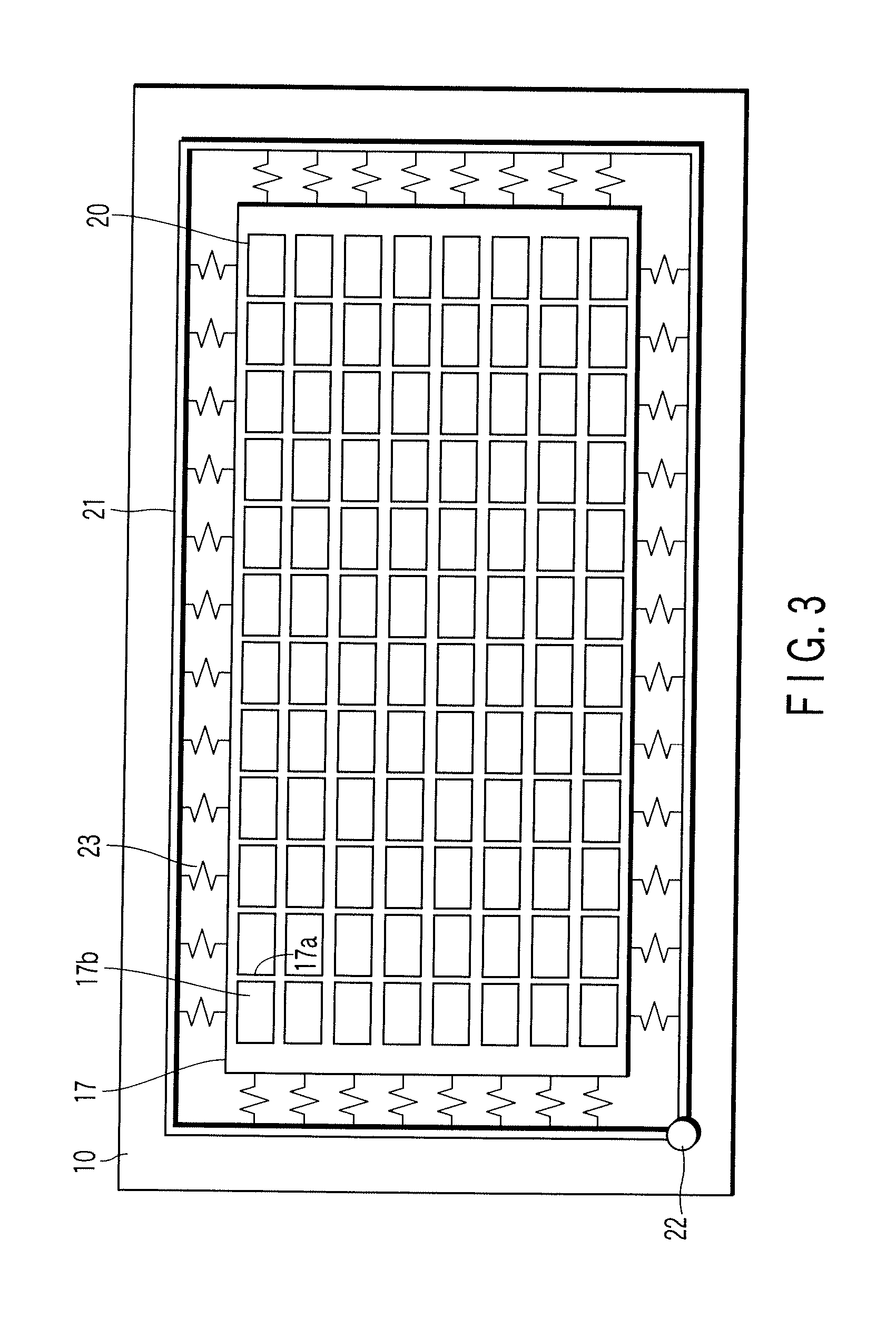
[0039] Thus, in this embodiment, a conducting part of the back-side substrate 12 opposite to the power supply wirings 21 and 21′ is covered by an insulating material, in order to prevent damage caused by an electric discharge occurring in the power supply wirings 21 and 21′. Hereinafter, an explanation will be given on a discharge control structure according to the invention with reference to FIG. 5. In the following explanation, it is assumed that a dividing structure of the metal back 17 is a two-dimensional structure shown in FIG. 3.

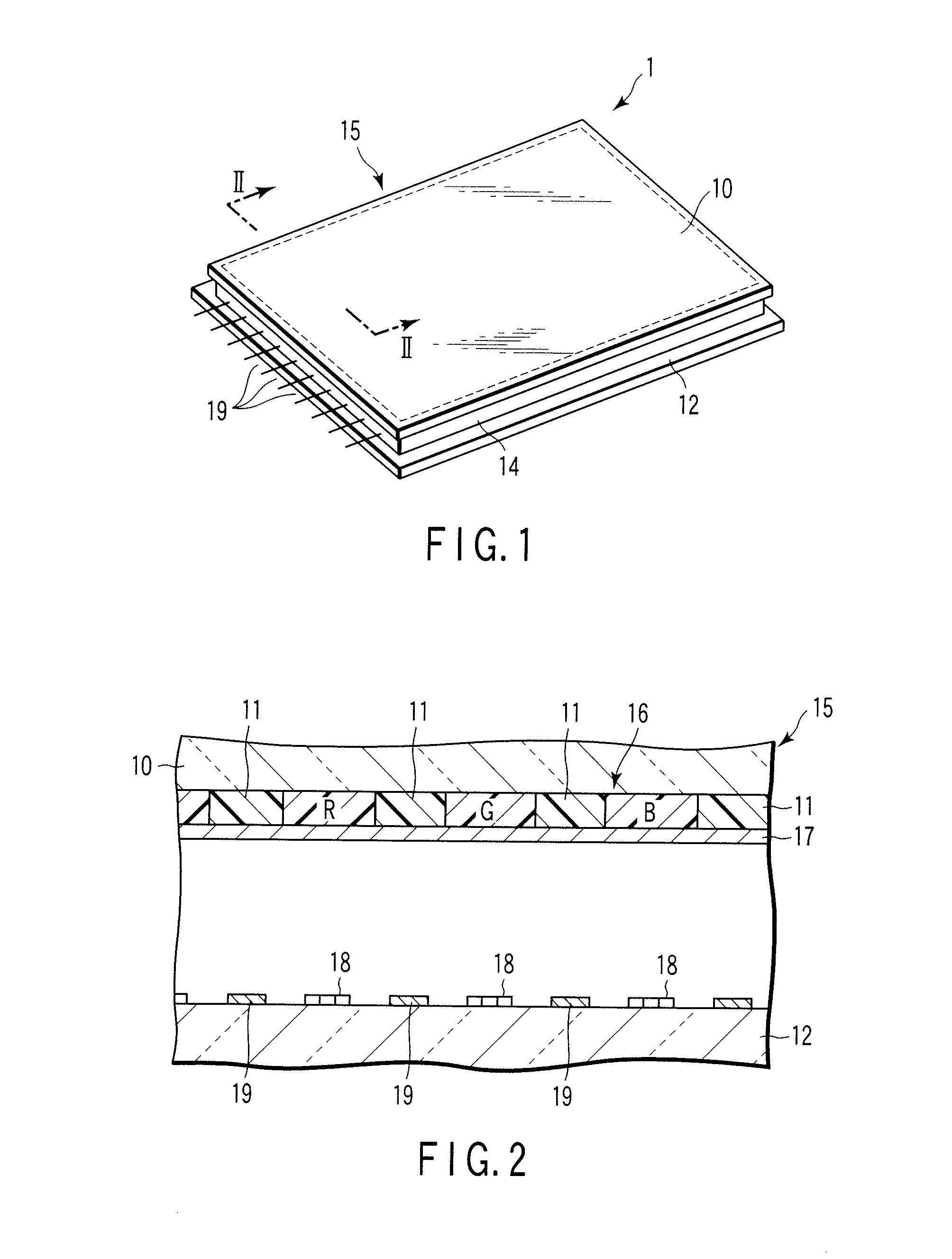
[0040] As shown in FIG. 5, on the inside surface of the back-side substrate 12, lower wires 19a (scanning wires) intersect at right angles with upper wires 19b (signal wires), forming a matrix pattern, with an insulating layer 25 interposed between the wires 19a and the wires 19b. The lower wire 19a and upper wire 19b function as a driving wire 19 mentioned before to selectively apply a driving voltage to the electron-emitting element 18. The ends of ...

second embodiment

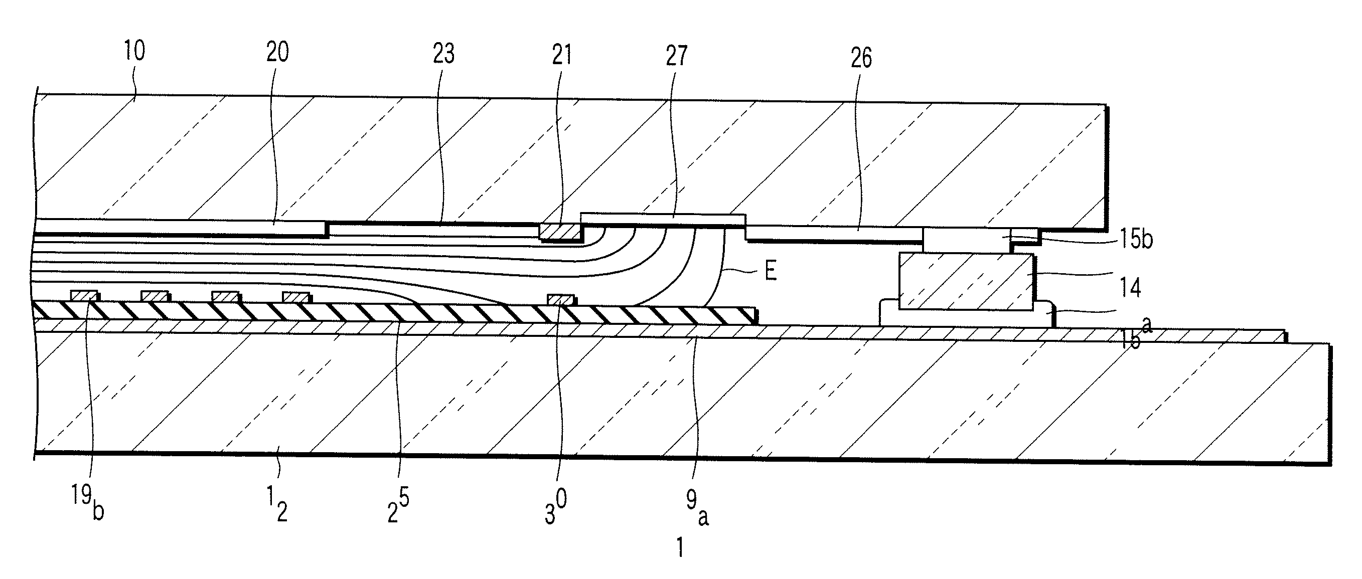
[0052] For example, the bypass member 30 to function as a lightning rod is grounded in the However, the bypass member 30 is given an optional potential. For example, by giving the bypass member 30 a potential of the value between the potential in the image display area 20 and the potential in the driving wire 19, an electric field shown as an equipotential line E in FIG. 9 can be formed around the bypass member 30. According to FIG. 9, the equipotential line E is coarse in the area around the power supply wiring 21, compared with the area close to the image display area 20, and it is seen that the probability of electric discharge is decreased in the area around the power supply wiring 21.

[0053] In the second embodiment, the bypass member 30 electrically independent of the driving wire 19 is provided through the insulating layer 25 (28). However, the bypass member 30 for escaping a discharge current may be provided between the power supply wiring 21 and driving wire 19. The insulat...


PUM


Abstract

An SED is formed by sealing a front-side substrate provided with an image display area having a fluorescent layer on its inside surface, and a back-side substrate provided with a plurality of electron-emitting elements and driving wires for driving the electron-emitting elements, through a rectangular frame-like sidewall. On the outside of the image display area of the front-side substrate, frame-like power supply wiring to apply a high voltage to the image display area through a metal back is formed. In the area of the back-side substrate opposite to the power supply wiring, a bypass member to function as a lightning rod is provided electrically independent of a lower wire.

Description

CROSS REFERENCE TO RELATED APPLICATIONS [0001] This is a Continuation Application of PCT Application No. PCT / JP2005 / 009541, filed May 25, 2005, which was published under PCT Article 21(2) in Japanese. [0002] This application is based upon and claims the benefit of priority from prior Japanese Patent Application No. 2004-180954, filed Jun. 18, 2004, the entire contents of which are incorporated herein by reference.BACKGROUND OF THE INVENTION [0003] 1. Field of the Invention [0004] The present invention relates to a flat display unit, which has a flat-panel vacuum enclosure, and excites and lights a fluorescent layer provided on a front-side substrate by emitting electrons from electron-emitting elements provided on a rear-side substrate. [0005] 2. Description of the Related Art [0006] Recently, a flat display unit such as a field emission display (FED) and a plasma display (PDP) has become known as a display unit having a flat-panel vacuum enclosure. As a kind of FED, a surface-condu...

Claims


Application Information

Patent Timeline
IPC IPC(8): G09G3/10H01J63/04H01J1/62H01J29/00H01J29/02H01J29/08H01J31/12
CPCH01J29/003H01J29/02H01J29/08H01J2329/00H01J1/30H01J31/12
Inventor YOKOTA, MASAHIROMURATA, HIROTAKANISHIMURA, TAKASHI
Owner KK TOSHIBA
Why Eureka
Try Eureka