
Method of processing a substrate and apparatus processing the same

Active Publication Date: 2007-04-12
TOKYO ELECTRON LTD
View PDF3 Cites 18 Cited by
  • Summary
  • Abstract
  • Description
  • Claims
  • Application Information

AI Technical Summary

Benefits of technology

[0010] The present invention contemplates a method of processing a wafer and apparatus processing the same that ensures that a liquid which is applied on a substrate to be processed and adheres to the substrate at a peripheral edge is removed, and that also allows the substrate to be processed within a reduced period of time and can also prevent the liquid from again adhering to the substrate.

Problems solved by technology

However, if the former method is applied, i.e., if as described in Japanese Patent Laying-Open No. 2003-045788, a wafer having resist applied thereon and dried is subsequently supplied at its back surface with a cleaning liquid to remove the resist, a long period of time may be required to remove the resist adhering to the wafer at a peripheral edge and the cleaning liquid may remain on the wafer.
In particular, if the cleaning liquid is for example cyclohexanone (C6H10O) a long period of time is required to remove the resist.
Furthermore, for the latter method, i.e., as disclosed in Japanese Patent Laying-Open No. 08-264412, the cleaning liquid running round the wafer and reaching its front, peripheral edge causes the resist to scatter and again adhere to the wafer, resulting in reduced product yields.
If the EBR process is not performed, however, an arm holding the wafer may be contaminated by the resist, which may again adhere to the wafer.

Method used


Image

  • Method of processing a substrate and apparatus processing the same
  • Method of processing a substrate and apparatus processing the same
  • Method of processing a substrate and apparatus processing the same

Examples


example

[0076] The above described resist application apparatus with the substrate processing apparatus of the present invention applied thereto and a conventional resist application apparatus were compared in an experiment in a resist removal process and in how long they take to perform the process.

[0077] Conditions for the Experiment

[0078] Resist: PAR (product name)

[0079] Solvent: cyclohexanone (C6H10O)

[0080] Flow rate for bevel-rinsing: 100 ml / min (in total for two nozzles)

[0081] Flow rate for back-rinsing: 100 ml / min (in total for two nozzles)

[0082] Under the above indicated conditions the experiment was conducted. The conventional apparatus provided a result as shown in Table 1 and the present apparatus provided a result as shown in Table 2.

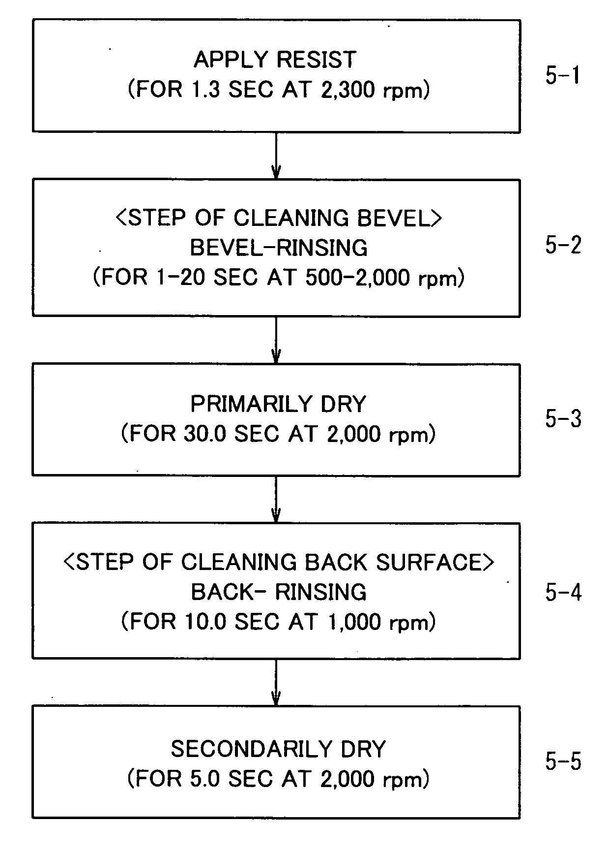
TABLE 1AccelerationSTEPTime (s)Speed (rpm)(rpm / s)Dispense11.32,30010,000resist212,30010,0003502,00010,00041201,00010,000back-rinsing*)511,00010,000652,00010,000

*) EBR arm drive time

[0083]

TABLE 2AccelerationSTEPTime (s)Speed (rpm)(rpm / s)Dispe...


PUM


Abstract

A spin chuck rotatably holds a semiconductor wafer, while resist is dropped on a surface of the semiconductor wafer through a resist application nozzle and thus applied thereon, and before the resist applied on the wafer dries, a cleaning liquid is supplied through a bevel cleaning nozzle to a portion of the wafer located at a peripheral portion thereof in a vicinity of a beveled portion to remove the resist adhering to the beveled portion. Thereafter, a film of the resist that is formed on the surface of the wafer is dried.

Description

BACKGROUND OF THE INVENTION [0001] 1. Field of the Invention [0002] The present invention relates generally to methods of processing substrates and apparatuses processing substrates and particularly to such methods and apparatuses for example applying resist for example on a semiconductor wafer and removing an excess of the resist that adheres to the wafer at a peripheral edge. [0003] 2. Description of the Background Art [0004] Generally in fabricating a semiconductor device a semiconductor wafer (hereinafter simply referred to as a “wafer”) is provided thereon with a thin film formed of indium tin oxide (ITO), an electrode pattern and the like, and to do so, photolithography is employed. In photolithography, photoresist is applied on a wafer to form a film of the resist which is in turn exposed to light in accordance with a predetermined circuit pattern which is in turn developed to form the circuit pattern in the film of the resist. [0005] In such photolithography process when the...

Claims


Application Information

Patent Timeline
IPC IPC(8): B05D3/10B05D3/04B05C13/02B08B3/00
CPCG03F7/162G03F7/168H01L21/67051H01L21/6715
Inventor FUKUDA, YOSHITERUOGATA, NOBUHIROISHII, TAKAYUKITANOUCHI, KEIJI
Owner TOKYO ELECTRON LTD
Features
  • Generate Ideas
  • Intellectual Property
  • Life Sciences
  • Materials
  • Tech Scout
  • Unparalleled Data Quality
  • Higher Quality Content
  • 60% Fewer Hallucinations
Learn More