Semiconductor device and manufacturing method thereof

a semiconductor device and manufacturing method technology, applied in the direction of semiconductor devices, basic electric elements, electrical equipment, etc., can solve the problems of electrical stress migration of copper wiring at the bottom of via-holes, wiring, etc., to improve yield and increase the resistance against migration of semiconductor devices

Active Publication Date: 2007-04-12
RENESAS ELECTRONICS CORP
View PDF15 Cites 25 Cited by
  • Summary
  • Abstract
  • Description
  • Claims
  • Application Information

AI Technical Summary

Benefits of technology

[0016] According to the present invention, it is possible to raise the resistance against migration of the semiconductor device including a multi-layer wiring structure to improve the yield.

Problems solved by technology

However, if copper wirings are used, electromigration or stress migration of copper wirings at the bottom of via-holes, adapted for forming vias to be connected to the copper wirings, is becoming of a problem.

Method used


Image

  • Semiconductor device and manufacturing method thereof
  • Semiconductor device and manufacturing method thereof
  • Semiconductor device and manufacturing method thereof

Examples


Embodiment Construction

[0026] Referring to the drawings, a preferred embodiment of the present invention will be described in detail. Meanwhile, the same reference numerals are used to depict the same components and corresponding description is sometimes omitted for simplicity of the description.

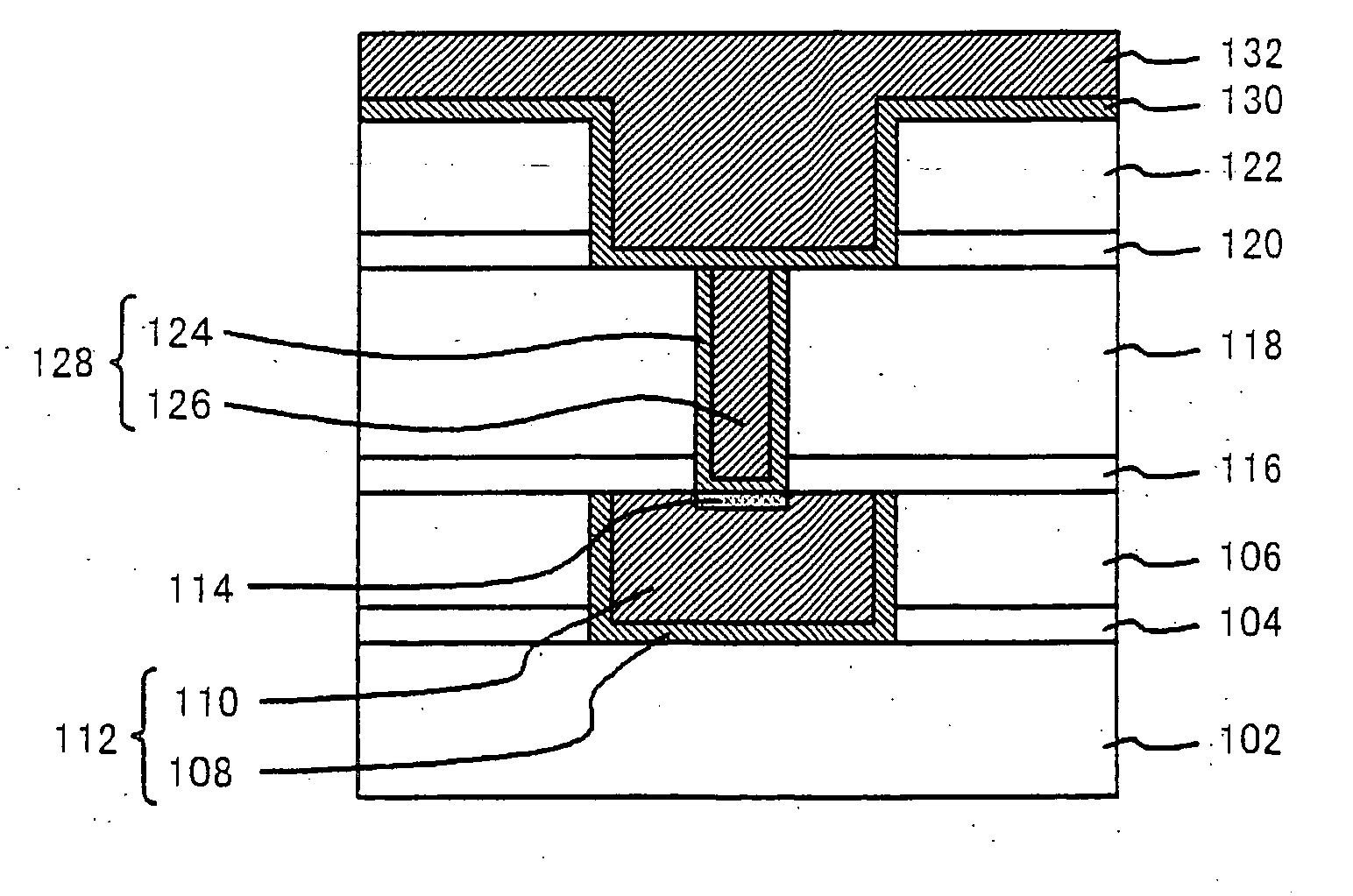
[0027]FIG. 1 depicts a cross-sectional view showing an example of the constitution of a semiconductor device of the instant embodiment.

[0028] A semiconductor device 100 includes a semiconductor substrate, not shown, on which there are formed an insulating film 102, a first etching stop film 104, a first interlayer insulating film 106, a barrier insulating film 116, a second interlayer insulating film 118, a second etching stop film 120 and a third interlayer insulating film 122, in this order. In the first etching stop film 104 and in the first interlayer insulating film 106, there is formed a first interconnect (wiring) 112 formed by a barrier metal film 108 and an interconnect (wiring) metal film 110. In the b...


PUM


Abstract

A semiconductor device has a multi-layer wiring in which resistance against migration of the semiconductor device is raised to improve the yield. Semiconductor device 100 includes a first interconnect (wiring) 112, formed in a first interlayer insulating film 106 on a semiconductor substrate, not shown, a via 128 provided on the first interconnect (wiring) 112 so that the via is connected to the first interconnect (wiring) 112, and a different element containing electrically conductive film 114. The different element containing electrically conductive film is formed selectively on a site on the top of the first interconnect (wiring) 112 where the first wiring is contacted with the bottom of the via 128. The different element containing electrically conductive film contains a metal of a main component of the first interconnect (wiring) 112 and a different element different from the metal of the main component.

Description

FIELD OF THE INVENTION [0001] This invention relates to a semiconductor device and a manufacturing method thereof. BACKGROUND OF THE INVENTION [0002] Recently, copper wirings (interconnects) have come to be used as metal wirings in semiconductor devices for decreasing the electrical resistance. However, if copper wirings are used, electromigration or stress migration of copper wirings at the bottom of via-holes, adapted for forming vias to be connected to the copper wirings, is becoming of a problem. Patent Document 1 discloses a technique comprising forming copper silicide on the top of a copper wiring formed by a copper-containing metal followed by forming a via thereon. This improves resistance against migration of the copper wiring. [0003] Patent Document 2 discloses a technique comprising exposing a layered structure, composed of a Cu film sandwiched between barrier films, to a silane gas, and selectively forming a copper silicide layer only on a portion of the wiring where cop...

Claims


Application Information

Patent Timeline
Patent Type & Authority Applications(United States)
IPC IPC(8): H01L21/44H01L31/00
CPCH01L21/76843H01L21/76849H01L21/76867H01L21/76886
Inventor KATOU, HIROAKI
Owner RENESAS ELECTRONICS CORP
Why Eureka
Try Eureka