Integrated circuit package system using etched leadframe

a leadframe and integrated circuit technology, applied in the direction of electrical equipment, semiconductor devices, semiconductor/solid-state device details, etc., can solve the problems of failure to use leadframes without tie bars or dam bars, defective wire bonding, etc., and achieve the effect of cost saving and versatility

Active Publication Date: 2007-04-19
STATS CHIPPAC LTD
View PDF12 Cites 34 Cited by
  • Summary
  • Abstract
  • Description
  • Claims
  • Application Information

AI Technical Summary

Benefits of technology

[0018] The present invention provides a versatile and cost effective system for manufacturing integrated circuit package systems.

Problems solved by technology

One problem that persists with leadframes is that as the integrated circuits are subject to miniaturization requiring integrated circuit packages having higher numbers of leads in intricate designs often including isolated heat sinks additional tie bars and dam bars are needed to hold these intricate design features together during manufacturing of the integrated circuit package.
However, the taping provides a cushioning effect that absorbs some of the ultrasonic energy transmitted during the wire bonding process resulting in defective wire bonding.
Attempts have been made to use leadframes without tie bars or dam bars, but have proven unsuccessful.
The grinding operation, however, introduces potentially harmful stresses, which can have an adverse effect on the function and reliability of the integrated circuit package.
Also, these attempts have been unable to provide a stable bonding platform for hanging heat sinks or leads during the wire bonding process.
This has resulted in design limitations for tie bar and dambar insertion, and the need for larger unusable space in leadframe designs.
Solutions to these problems have been long sought but prior developments have not taught or suggested any solutions and, thus, solutions to these problems have long eluded those skilled in the art.

Method used


Image

  • Integrated circuit package system using etched leadframe
  • Integrated circuit package system using etched leadframe
  • Integrated circuit package system using etched leadframe

Examples


Embodiment Construction

[0031] In the following description, numerous specific details are given to provide a thorough understanding of the invention. However, it will be apparent that the invention may be practiced without these specific details. In order to avoid obscuring the present invention, some well-known system configurations and process steps are not disclosed in detail.

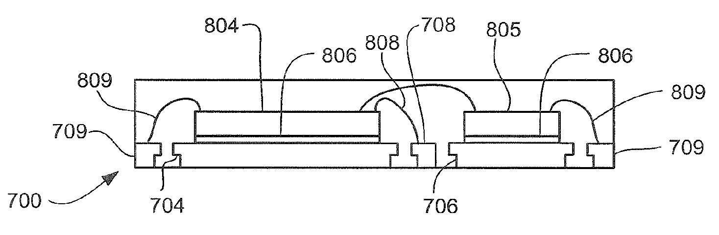
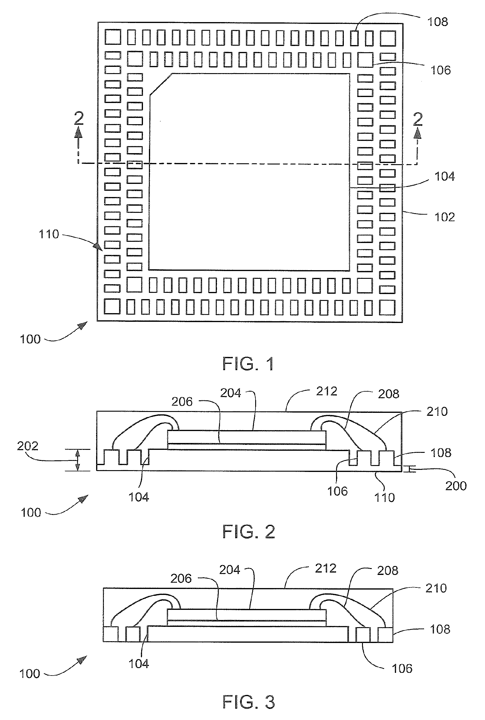
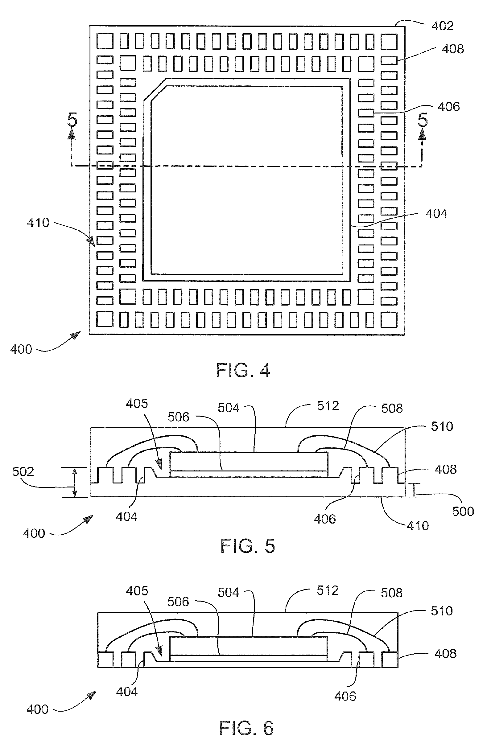
[0032] Likewise, the drawings showing embodiments of the device are semi-diagrammatic and not to scale and, particularly, some of the dimensions are for the clarity of presentation and are shown greatly exaggerated in the FIGs.

[0033] The term “horizontal” as used herein is defined as a plane parallel to the conventional plane or surface of the leadframe, regardless of its orientation. The term “vertical” refers to a direction perpendicular to the horizontal as just defined. Terms, such as “on”, “above”, “below”, “bottom”, “top”, “side” (as in “sidewall”), “higher”, “lower”, “over”, and “under”, are defined with respect to the ho...


PUM


Abstract

An integrated circuit package system includes a conductive substrate. A heat sink and a plurality of leads are etched in the substrate to define a conductive film connecting the heat sink and the plurality of leads to maintain their spatial relationship. A die is attached to the heat sink and wire bonded to the plurality of leads. An encapsulant is formed over the die, the heat sink, and the plurality of leads. The conductive film is etched away to expose the encapsulant and the bottom surfaces of the heat sink and the plurality of leads. Wave soldering is used to form solder on at least the plurality of leads. Multiple heat sinks and hanging leads are provided.

Description

TECHNICAL FIELD [0001] The present invention relates generally to integrated circuit manufacturing, and more particularly to a system for manufacturing a non-leaded integrated circuit package system. BACKGROUND ART [0002] In the electronics industry, the continuing goal has been to reduce the size of electronic devices such as camcorders and portable telephones while increasing performance and speed. Integrated circuit packages for complex systems typically are comprised of a multiplicity of interconnected integrated circuit chips. The integrated circuit chips usually are made from an integrated circuit material such as silicon or gallium arsenide. Integrated circuit devices are formed in various layers of the integrated circuit chips using photolithographic techniques. The integrated circuit chips may be mounted in packages that are then mounted on printed wiring boards. [0003] Integrated circuit packages including integrated circuit chips typically have numerous leads, or lead fin...

Claims


Application Information

Patent Timeline
Patent Type & Authority Applications(United States)
IPC IPC(8): H01L23/34
CPCH01L21/4832H01L23/49503H01L23/49582H01L2224/48091H01L2224/48137H01L2224/48247H01L2224/73265H01L2924/01078H01L2924/14H01L2924/00014H01L24/48H01L2224/32245H01L2224/45099H01L2924/00H01L2224/32257H01L2924/181H01L2924/18301H01L2924/00012
Inventor ONG, YOU YANGNG, CHEONG CHIANGMOHMAD, SUHAIRI
Owner STATS CHIPPAC LTD
Why Eureka
Try Eureka