Printed circuit board

a printed circuit board and printed circuit technology, applied in the direction of printed circuits, printed circuit details, printed circuits, etc., can solve problems such as defect formation in the soldering process, and achieve the effect of slowing down heat distribution and reducing defect formation

Inactive Publication Date: 2007-04-26
HON HAI PRECISION IND CO LTD
View PDF2 Cites 8 Cited by
  • Summary
  • Abstract
  • Description
  • Claims
  • Application Information

AI Technical Summary

Benefits of technology

[0005] An exemplary printed circuit board includes a reference layer, a through hole defined in the reference layer, and a plurality of insulating areas are defined in the reference layer around the through hole. The copper around the through hole is separated by the insulating areas and forms a plurality of copper strips. The metal area around the through hole available for heat dissipation is reduced to slow down heat distribution. Thus, defect formation is reduced when the PCB is in the reflow process.

Problems solved by technology

However, rapid heat dissipation leads to defect formation in the soldering process.

Method used


Image

  • Printed circuit board
  • Printed circuit board
  • Printed circuit board

Examples


Embodiment Construction

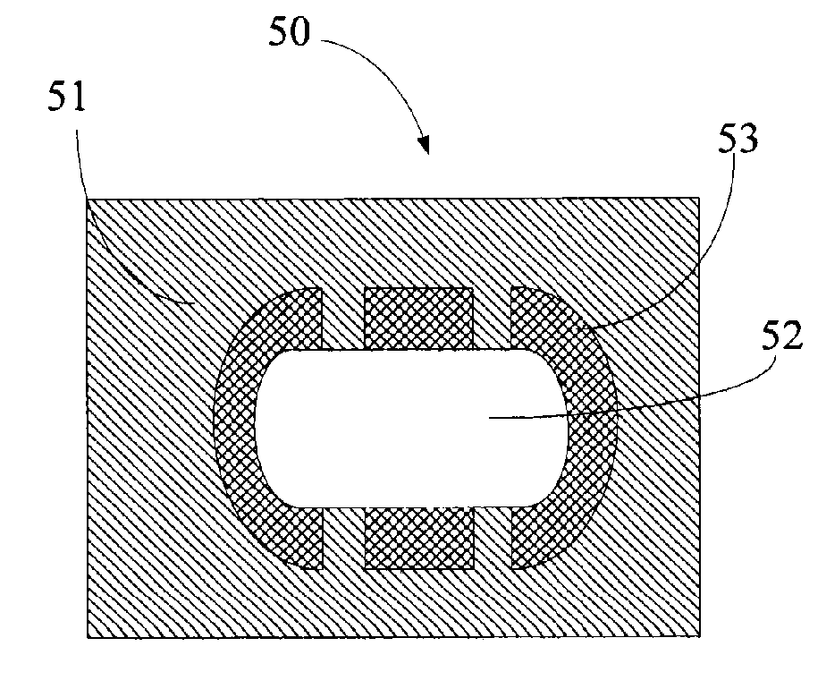
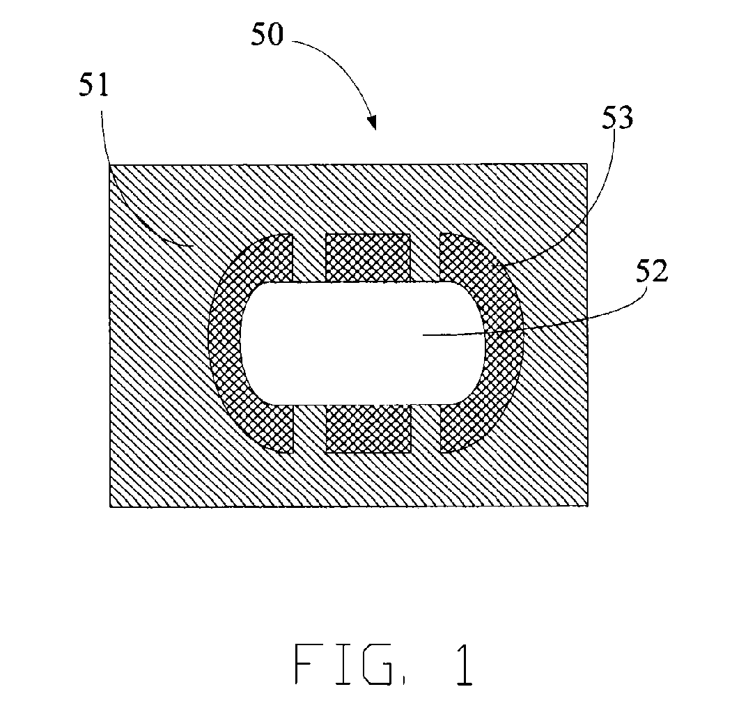
[0009] Referring to FIG. 1, a reference plane of a printed circuit board (PCB) according to a preferred embodiment of the present invention is provided. The PCB 50 includes a reference layer 51, a through hole 52, and a plurality of etched insulating areas 53 surrounding the through hole 52. The through hole 52 is generally ellipse shaped. The reference plane 51 is a solid copper layer. The copper around the through hole 52 is separated by the insulating areas 53 and forms a plurality of copper strips. The reference layer 51 is electrically connected to the components inserted in the through hole 52 by the copper strips. Preferably, a width of the strips is approximately 14 mils, and a width of the insulating areas is approximately 15 mils.

[0010] In this embodiment the metal area around the through hole 52 available for heat dissipation is much smaller than on conventional PCBs, to slow down heat distribution. Defect formation is thus reduced when the PCB is in a reflow process.

[0...


PUM


Abstract

A printed circuit board includes a reference layer, a through hole defined in the reference layer, and a plurality of insulating areas are defined in the reference layer around the through hole. The copper around the through hole is separated by the insulating areas and forms a plurality of copper strips. The metal surface area around the through hole available for heat dissipation is reduced to slow down heat distribution. Defect formation is thus reduced when the PCB is in a reflow process.

Description

FIELD OF THE INVENTION [0001] The present invention relates to a printed circuit board. DESCRIPTION OF RELATED ART [0002] Multilayer printed circuit boards (PCBs) are commonly used in electronic devices to connect electronic components such as integrated circuits to one another. A typical multilayer PCB includes many layers of copper, with each layer of copper separated by a dielectric material. Generally, several of the copper layers are used to provide a reference voltage plane or ground plane. [0003] Referring to FIG. 2, a reference plane of a printed circuit board is provided. The printed circuit board 40 includes a reference layer 41, and a through hole 34. A component is mounted on the PCB 40 by inserting a lead through the through hole 34 in the PCB 40 and then soldering the lead in place on the opposite side of the PCB 40 during a reflow process. The lead of the component is electrically connected to the reference plane. The reference plane of the printed circuit board distr...

Claims


Application Information

Patent Timeline
Patent Type & Authority Applications(United States)
IPC IPC(8): H01R12/04H05K1/11
CPCH05K1/116H05K3/3447H05K3/429H05K2201/062H05K2201/093H05K2201/0969H05K2201/09854
Inventor HUANG, YA-LING
Owner HON HAI PRECISION IND CO LTD
Why Eureka
Try Eureka