Light emitting diode package and method of manufacturing the same

a technology of light-emitting diodes and packaging, which is applied in the direction of optical articles, solid-state devices, other domestic articles, etc., can solve the problems of decreasing light efficiency and reducing transmittance, and achieve excellent physical stability

Active Publication Date: 2007-05-03
SUZHOU LEKIN SEMICON CO LTD
View PDF23 Cites 41 Cited by
  • Summary
  • Abstract
  • Description
  • Claims
  • Application Information

AI Technical Summary

Benefits of technology

[0015] The invention provides an LED package with an excellent physical stability.

Problems solved by technology

Meanwhile, light emitted from the LED 210 is reflected a lot inside the mold lens 250, that is, internal reflection occurs a lot inside the mold lens, decreasing the transmittance and eventually decreasing the light efficiency.

Method used


Image

  • Light emitting diode package and method of manufacturing the same
  • Light emitting diode package and method of manufacturing the same
  • Light emitting diode package and method of manufacturing the same

Examples


Embodiment Construction

[0026] It will be understood that when an element is referred to as being ‘on’ a layer, it can be directly on the layer, and one or more intervening layers may also be present.

[0027] Reference will now be made in detail to the preferred embodiments of the present invention, examples of which are illustrated in the accompanying drawings.

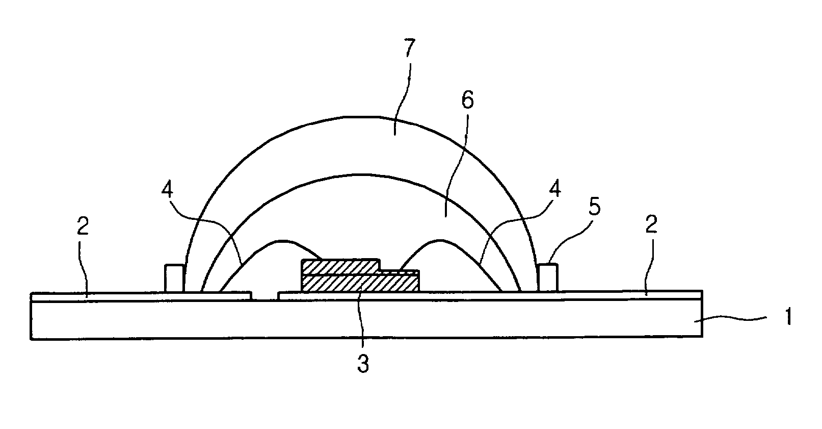
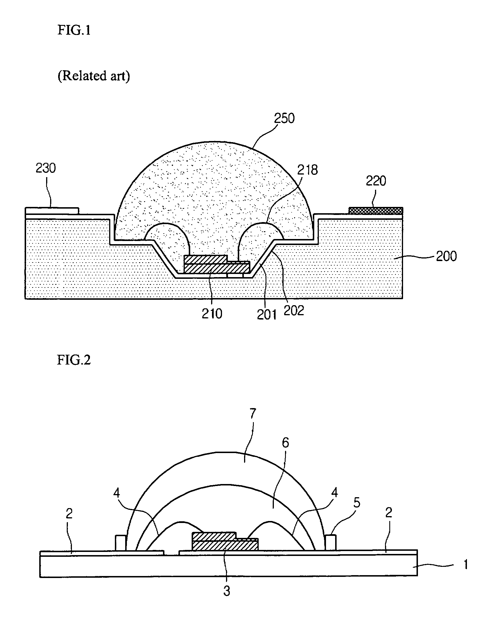
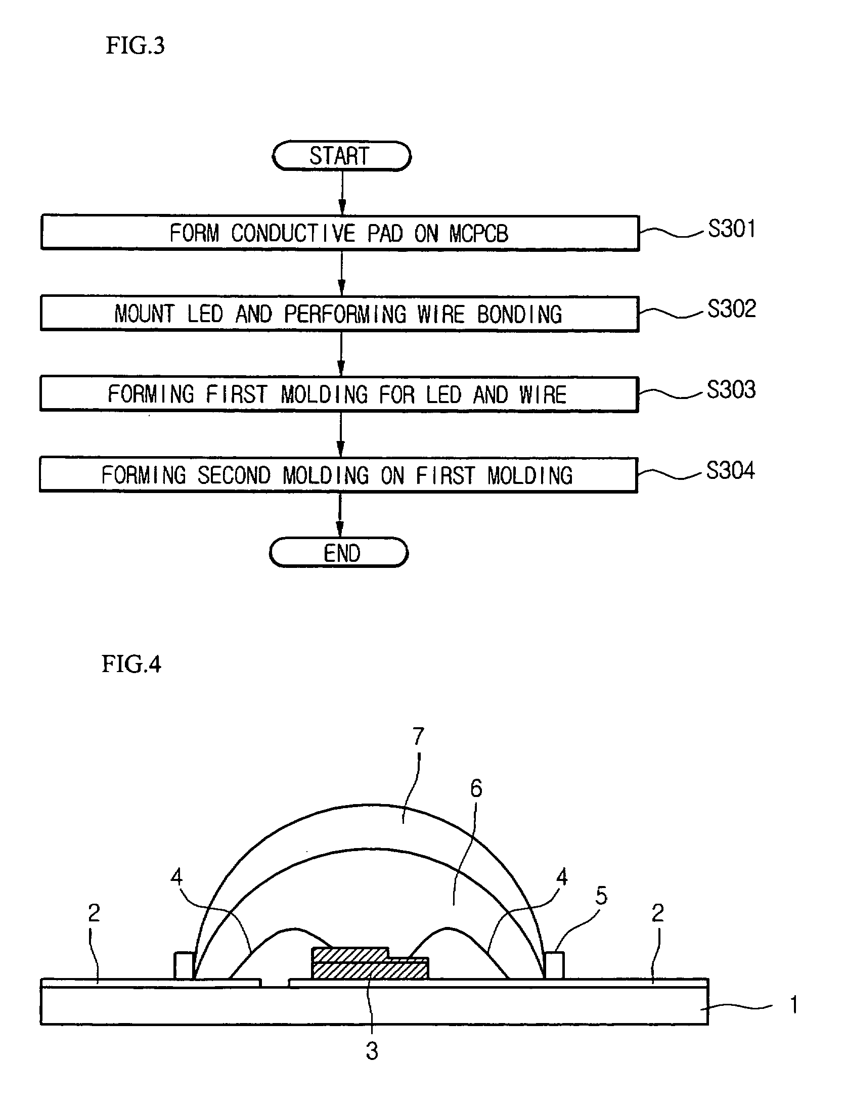
[0028]FIG. 2 is a sectional view of an LED package according to an embodiment of the present invention.

[0029] Referring to FIG. 2, the present invention exemplarily illustrates a SMD type LED package manufactured using a metal core printed circuit board (MCPCB) as an LED package.

[0030] An LED package according to an embodiment of the present invention includes an MCPCB 1, two electrode pads 2 formed on the MCPCB 1, an LED 3 formed on the electrode pads 2, two wires 4 connecting the LED 3 with the electrode pads 2, and a first molding 6 formed outside the LED 3 and the wires 4 and a second molding 7 formed outside the first molding 6.

[0031] The LE...


PUM

PropertyMeasurementUnit
RIaaaaaaaaaa
RIaaaaaaaaaa
RIaaaaaaaaaa

Abstract

A light emitting diode (LED) package is provided. The LED package includes a printed circuit board (PCB), an electrode pad, an LED, a wire, and first and second moldings. The electrode pad and the LED are formed on the PCB. The wire electrically connects the LED with the electrode pad. The first molding is formed on the LED and the second molding is formed on the first molding.

Description

BACKGROUND OF THE INVENTION [0001] 1. Field of the Invention [0002] The present invention relates to a light emitting diode package and a method of manufacturing the same. [0003] 2.Description of the Related Art [0004] A light emitting diode (LED) is a semiconductor device that can realize a light source of various colors using a compound semiconductor material such as GaAs, AlGaAs, GaN, InGaN, and AlGaInP. [0005] Generally, color, brightness, luminosity, etc. determine a characteristic of an LED. The characteristic of the LED is generally determined by a compound semiconductor material used in the LED, but is greatly influenced by a package structure for mounting chips. [0006] In particular, as information telecommunication devices have become small-sized and slim, elements such as a resistor, a condenser, and a noise filter have become small-sized even more and been directly mounted in a printed circuit board (PCB) (a surface mount device (SMD) type). [0007]FIG. 1 is a view illust...

Claims


Application Information

Patent Timeline
Patent Type & Authority Applications(United States)
IPC IPC(8): H01L33/00H01L33/54H01L33/56H01L33/62
CPCB29C39/025B29C39/026B29C39/10B29L2011/00H01L2224/48091H01L33/54H01L2924/00014
Inventor PARK, BO GEUN
Owner SUZHOU LEKIN SEMICON CO LTD
Why Eureka
Try Eureka