Light emitting diode package

a technology of light-emitting diodes and led packages, which is applied in the direction of printed circuit aspects, printed circuit boards, basic electric elements, etc., can solve the problem of limited useable space of conventional led packages, and achieve the effect of enhancing the flexibility of led packages in various spaces

Inactive Publication Date: 2007-05-03
CHIPMOS TECH INC
View PDF5 Cites 79 Cited by
  • Summary
  • Abstract
  • Description
  • Claims
  • Application Information

AI Technical Summary

Benefits of technology

[0018] Based on the above described, the LED package in the present invention features a flexible carrier therein, which enables the LED package to possess yieldingness, therefore the usage flexibility of the LED package in various spaces is enhanced.

Problems solved by technology

Note that, when a plurality of LED chips are packed on a single carrier, since the carrier in the LED package is a rigid carrier, or the carrier is not flexible, the useable space of the conventional LED package is limited.
Thus, how to make a LED package flexible for increasing the useable space thereof to adapt the compactness trend of modern electronic products is an important issue.

Method used


Image

  • Light emitting diode package
  • Light emitting diode package
  • Light emitting diode package

Examples


Embodiment Construction

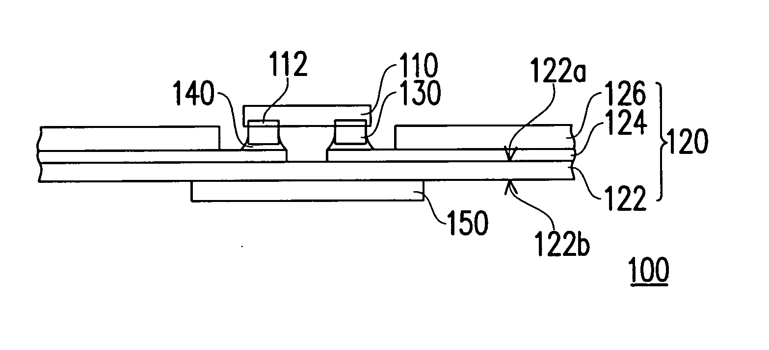
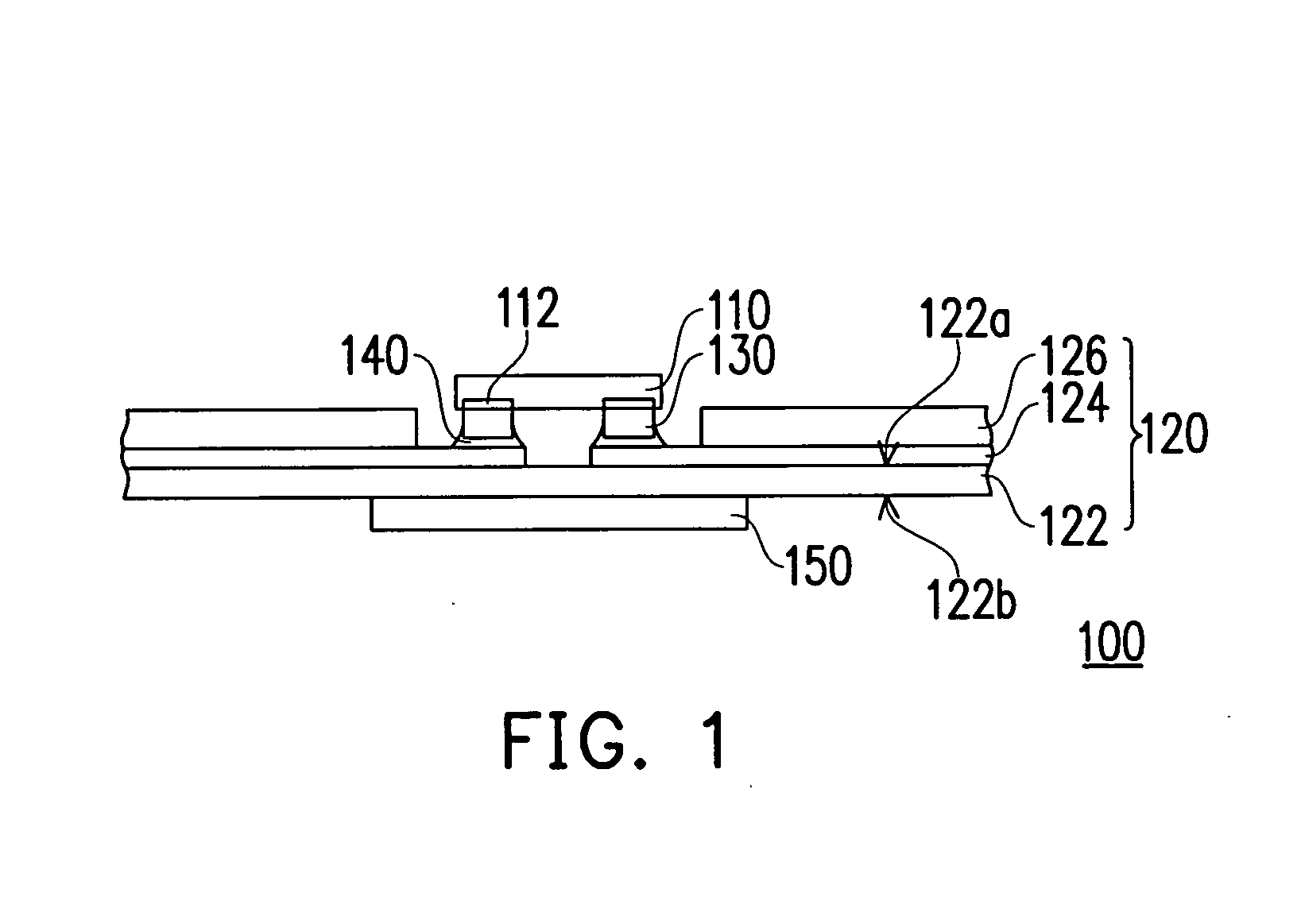
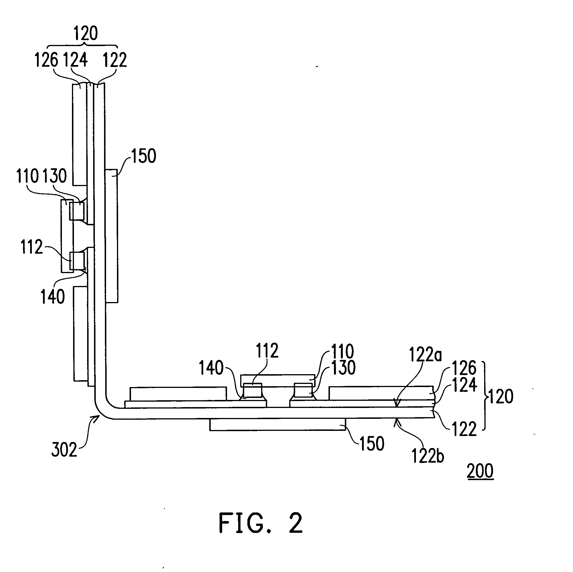
[0022]FIG. 1 is a diagram of a LED package provided by the first embodiment of the present invention. It can be seen from FIG. 1 that the LED package 100 of the present embodiment includes a LED chip 110 and a flexible carrier 120, wherein the LED chip 110 has a plurality of electrodes 112. The flexible carrier 120 has a flexible substrate 122 and a circuit layer 124, the flexible substrate 122 has a support surface 122a and a back surface 122b opposite the support surface 122a, and the circuit layer 124 is disposed on the support surface 122a.

[0023] On the other hand, the LED package 100 further includes a plurality of bumps 130, wherein the bumps 130 are disposed on the electrodes 112, while the circuit layer 124 is electrically connected to the electrodes 112 through the bumps 130. Herein, the bump 130 is, for example, a gold bump, a copper bump, a nickel bump or an aluminum bump and the material of the circuit layer 124 is, for example, copper. In the embodiment, the flexible c...


PUM


Abstract

A LED package includes a LED chip and a flexible carrier, wherein the LED chip has a plurality of electrodes. The flexible carrier has a flexible substrate and a circuit layer, wherein the flexible substrate has a support surface and a back surface opposite the support surface, and the circuit layer is disposed on the support surface. In addition, the LED package further includes a plurality of bumps and the electrodes of the LED chip are electrically connected to the circuit layer of the flexible carrier through the bumps.

Description

CROSS-REFERENCE TO RELATED APPLICATION [0001] This application claims the priority benefit of Taiwan application serial no. 094137764, filed on Oct. 28, 2005. All disclosure of the Taiwan application is incorporated herein by reference. BACKGROUND OF THE INVENTION [0002] 1. Field of Invention [0003] The present invention relates to a semiconductor package, and particularly to a light emitting diode package (LED package). [0004] 2. Description of the Related Art [0005] A light emitting diode (LED) formed by semiconductor material made of the compound of the group III-V elements is a broad band-gap luminous component, which emits lights from infrared light to ultraviolet light, including all wavebands of visible light. In recent years, along with the rapid progress in high-brightness gallium nitride (GaN) LED producing blue / green light, full-color LED displays, white LEDs and LED traffic lights have gained feasible applications, while other kinds of LEDs have also got popular applicat...

Claims


Application Information

Patent Timeline
Patent Type & Authority Applications(United States)
IPC IPC(8): H01L23/495
CPCH01L33/483H01L33/62H01L33/64H01L2224/16H01L2924/01079H05K1/189H05K3/0058H05K2201/10106H05K2201/2009H01L2224/05571H01L2224/05573H01L2924/00014H01L2224/05599
Inventor WANG, JIUN-HENG
Owner CHIPMOS TECH INC
Why Eureka
Try Eureka