Method and apparatus for varying the programming duration and/or voltage of an electrically floating body transistor, and memory cell array implementing same

a technology of electrical floating body transistors and programming durations, applied in the field of semiconductor memory cells, arrays, architecture and devices, can solve the problems of additional source of charge degradation, leakage and recombination

Active Publication Date: 2007-05-03
MICRON TECH INC
View PDF4 Cites 127 Cited by
  • Summary
  • Abstract
  • Description
  • Claims
  • Application Information

AI Technical Summary

Benefits of technology

[0023] There are many inventions described and illustrated herein. The present inventions are neither limited to any single aspect nor embodiment thereof, nor to any combinations and/or permutations of such aspects and/or embodiments. Moreover, each of the aspects of the present

Problems solved by technology

Notably, an additional source of charge degra

Method used


Image

  • Method and apparatus for varying the programming duration and/or voltage of an electrically floating body transistor, and memory cell array implementing same
  • Method and apparatus for varying the programming duration and/or voltage of an electrically floating body transistor, and memory cell array implementing same
  • Method and apparatus for varying the programming duration and/or voltage of an electrically floating body transistor, and memory cell array implementing same

Examples


Embodiment Construction

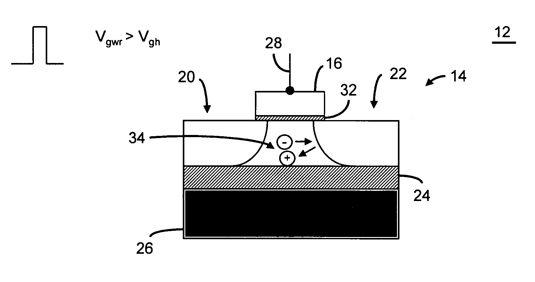
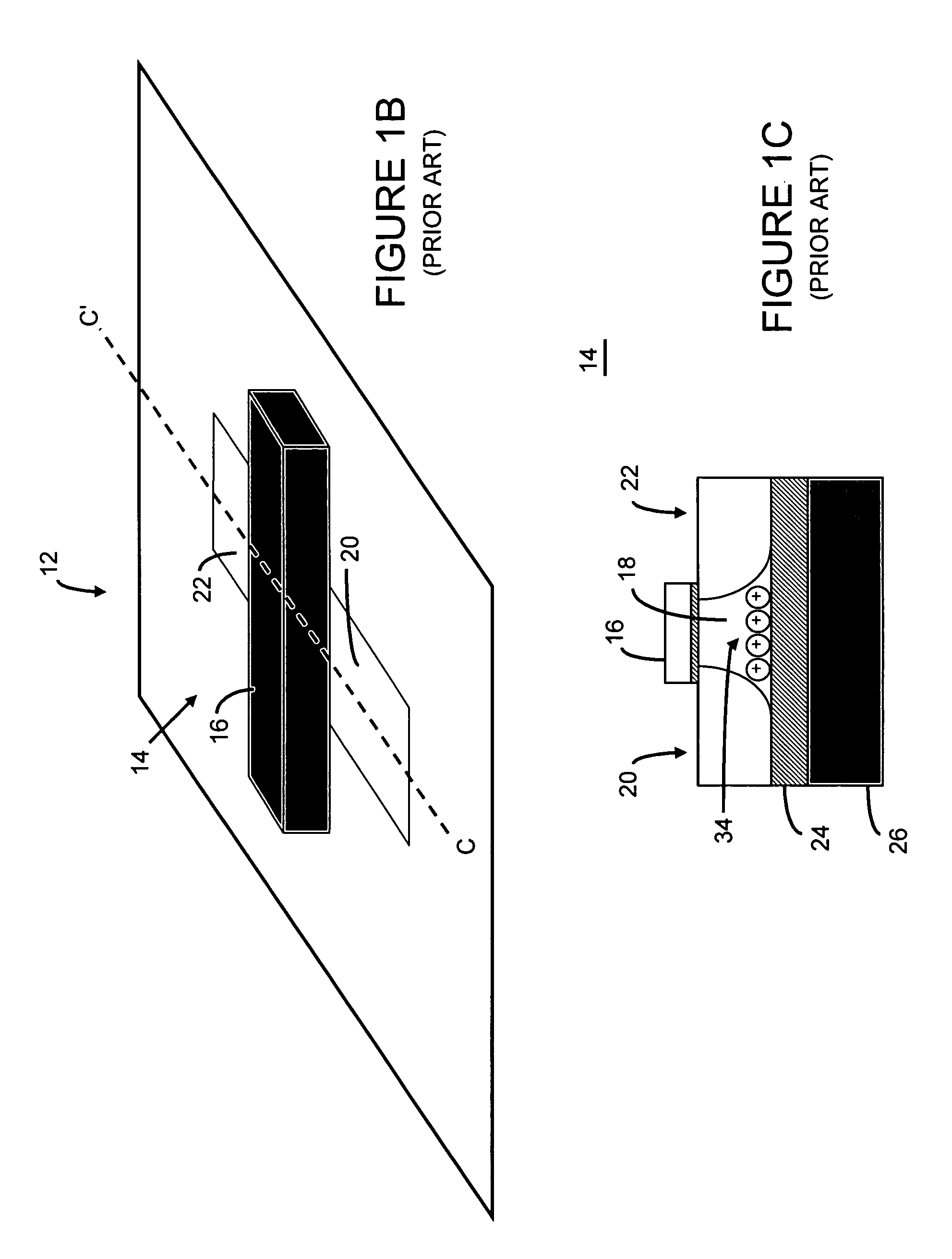
[0062] At the outset, it should be noted that there are many inventions described herein as well as many aspects and embodiments of those inventions. The present inventions are directed to circuitry and techniques for reading, writing and / or operating a semiconductor memory cell, array, architecture and device including electrically floating body transistors in which an electrical charge is stored in the body of the transistor. The present inventions are also directed to semiconductor memory cell, array, architecture and device that implement such circuitry and techniques. Notably, the memory cell and / or memory cell array may comprise a portion of an integrated circuit device, for example, logic device (such as, for example, a microcontroller or microprocessor) or a portion of a memory device (such as, for example, a discrete memory).

[0063] In particular, in one aspect, the present inventions are directed to independently controllable parameters, for a given memory operation (for e...


PUM


Abstract

There are many inventions described herein as well as many aspects and embodiments of those inventions, for example, circuitry and techniques for reading, writing and/or operating a semiconductor memory cells of a memory cell array, including electrically floating body transistors in which an electrical charge is stored in the body of the transistor. In one aspect, the present inventions are directed to one or more independently controllable parameters of a memory operation (for example, restore, write, refresh), to program or write a data state into a memory cell. In one embodiment, the parameter is the amount of time of programming or writing a predetermined data state into a memory cell. In another embodiment, the controllable parameter is the amplitude of the voltage of the control signals applied to the gate, drain region and/or source region during programming or writing a predetermined data state into a memory cell. Indeed, the controllable parameters may be both temporal and voltage amplitude. Notably, the memory cell array may comprise a portion of an integrated circuit device, for example, logic device (for example, a microprocessor) or a portion of a memory device (for example, a discrete memory).

Description

RELATED APPLICATION [0001] This application claims priority to: (1) U.S. Provisional Application Ser. No. 60 / 731,668, entitled “Method and Apparatus for Varying the Programming Duration of a Floating Body Transistor, and Memory Cell, Array, and / or Device Implementing Same”, filed Oct. 31, 2005, and (2) U.S. Provisional Application Ser. No. 60 / 736,613, entitled “Method and Apparatus for Varying the Programming Duration of a Floating Body Transistor, and Memory Cell, Array, and / or Device Implementing Same”, filed Nov. 14, 2005. The contents of these provisional applications are incorporated by reference herein in their entirety.BACKGROUND [0002] The inventions relate to a semiconductor memory cell, array, architecture and device, and techniques for controlling and / or operating such cell, array and device; and more particularly, in one aspect, to a dynamic random access memory (“DRAM”) cell, array, architecture and device, wherein the memory cell includes an electrically floating body ...

Claims


Application Information

Patent Timeline
IPC IPC(8): G11C7/10
CPCG11C5/025G11C7/14G11C7/22G11C11/404G11C11/406G11C11/4074G11C11/4076G11C11/4099G11C2211/4016G11C2211/4061G11C2211/4068
Inventor POPOFF, GREGORY ALLANCHAMPS, PAUL DEDAGHIGHIAN, HAMID
Owner MICRON TECH INC
Why Eureka
Try Eureka