
IC card

Inactive Publication Date: 2007-05-10
RENESAS ELECTRONICS CORP
View PDF28 Cites 6 Cited by
  • Summary
  • Abstract
  • Description
  • Claims
  • Application Information

AI Technical Summary

Benefits of technology

[0009] First, it became obvious that when Zener diodes of a large size are integrated on a semiconductor integrated circuit chip to obtain an energy withstand amount that helps reinforce the prevention of electrostatic damage, the area efficiency decreases in the midst of fine circuit elements, driving up the cost to a conspicuous degree.
[0054] Therefore, even in case the input circuit of the semiconductor integrated circuit chip is electrostatically damaged, the data that remain safe in the memory can be easily recovered.

Problems solved by technology

First, it became obvious that when Zener diodes of a large size are integrated on a semiconductor integrated circuit chip to obtain an energy withstand amount that helps reinforce the prevention of electrostatic damage, the area efficiency decreases in the midst of fine circuit elements, driving up the cost to a conspicuous degree.
Second, when an element for protection from an overvoltage is attached to the semiconductor integrated circuit chip to reinforce the prevention of electrostatic damage, the efficiency for preventing the electrostatic damage does not increase unless consideration is given to a relationship between the characteristics and the ability of the overvoltage protection circuit incorporated in the semiconductor integrated circuit chip.
Besides, the externally attached circuit elements that are large in size or that are large in number, cause an increase in the size and thickness of the IC card.
Third, even when the countermeasure against the electrostatic damage is taken by using the externally attached circuit elements, there is no guarantee that the device is absolutely safe from the damage when it is handled in an unexpected manner by a person who is not familiar with.

Method used


Image

  • IC card
  • IC card
  • IC card

Examples


Embodiment Construction

[0082] First, described below is a principle for reinforcing the function for preventing electrostatic damage to the semiconductor integrated circuit by using externally attached circuit elements such as varistors.

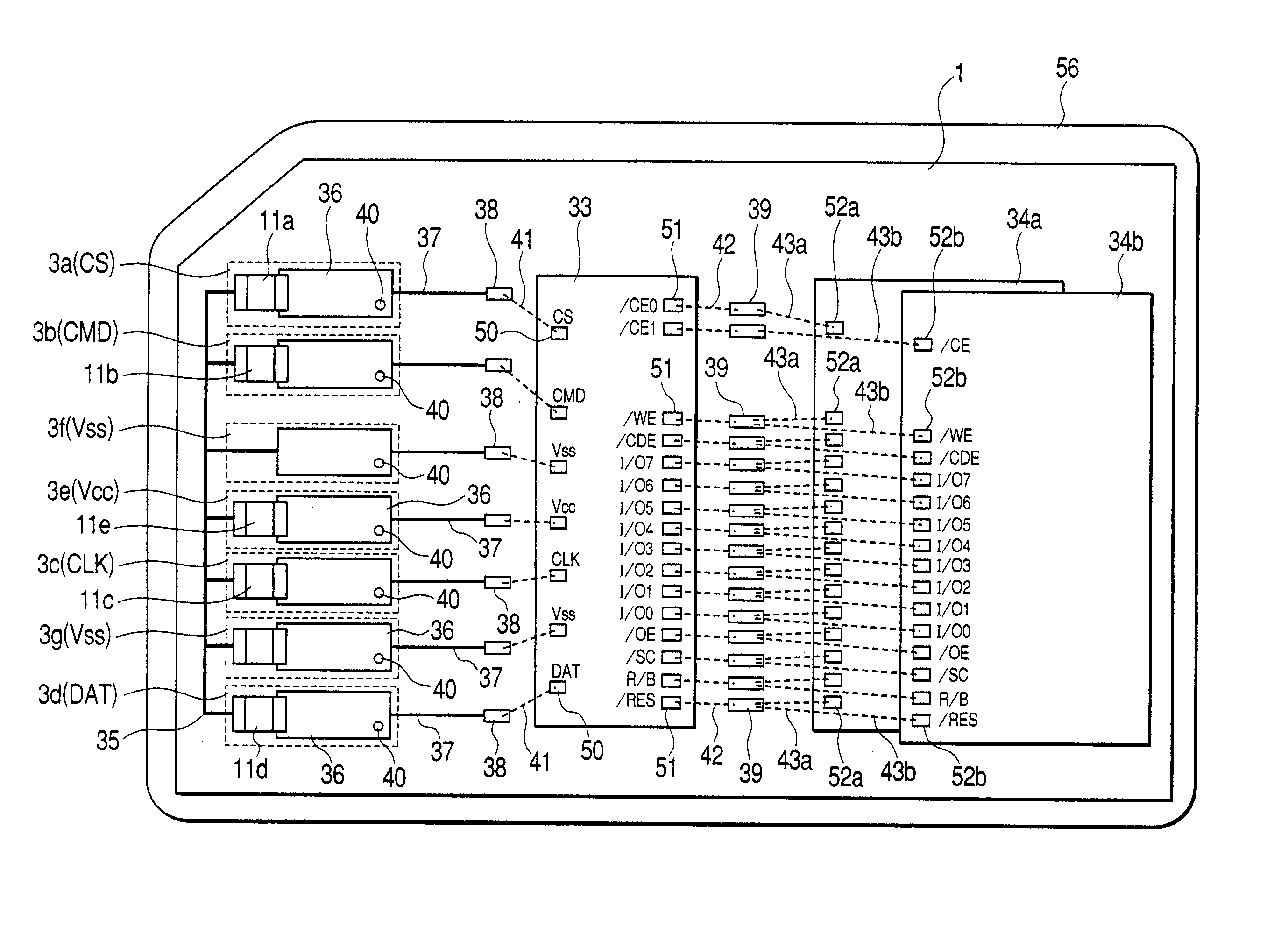
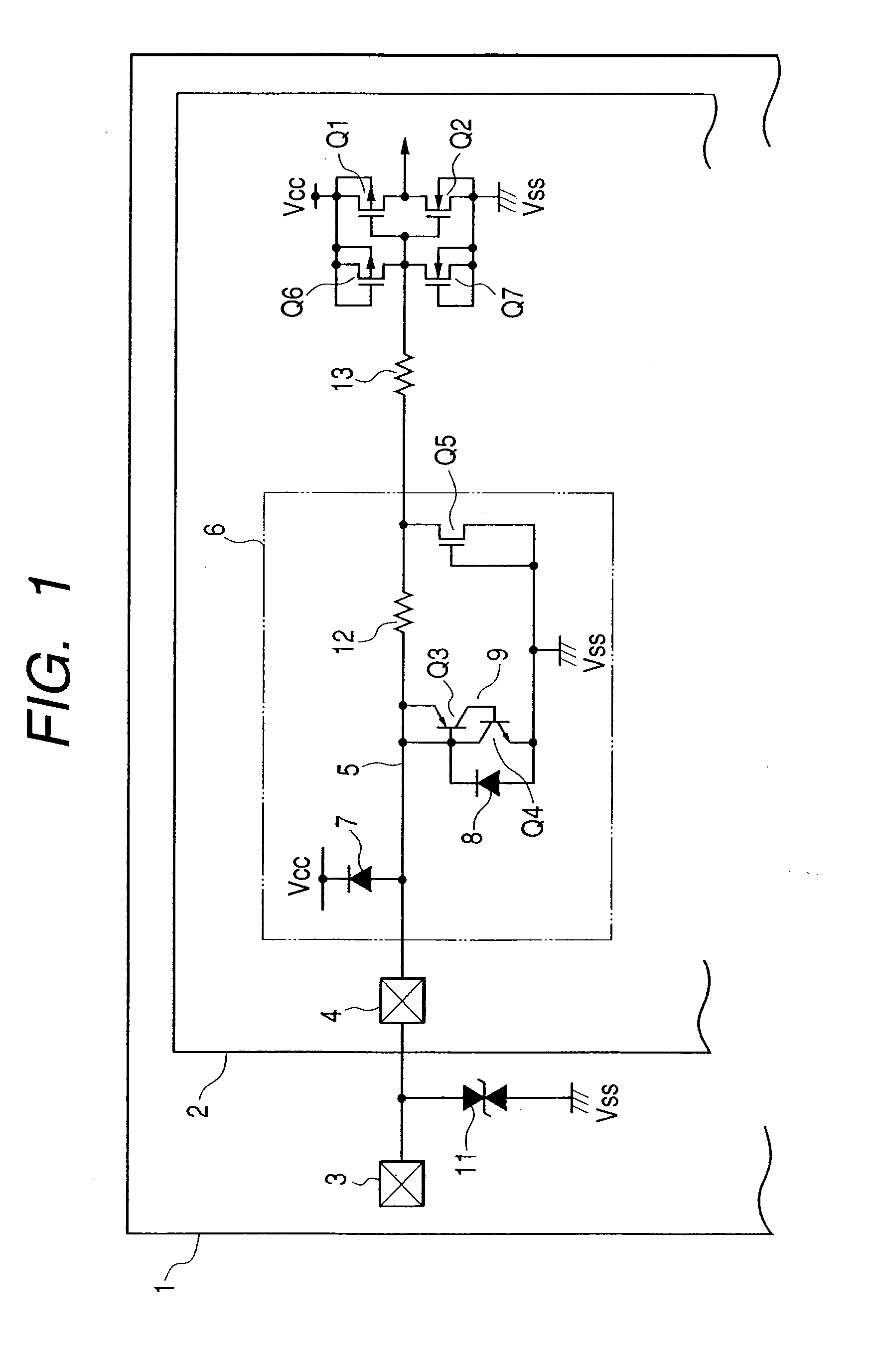
[0083]FIG. 1 illustrates a connection terminal of an IC card according to the invention. The IC card that is shown has a semiconductor integrated circuit chip 2 mounted on a card substrate 1, and, typically, has connection terminals 3 that are exposed. The connection terminals 3 are interface terminals for electrically connecting the IC card to a host unit to which the IC card is detachably attached.

[0084] The connection terminals 3 are connected to predetermined external terminals 4 of the semiconductor integrated circuit chip 2. The external terminals are input terminals which are connected to, for example, a CMOS inverter in the initial stage of the input circuit via signal lines 5. The CMOS inverter is constituted by a p-channel field-effect transistor (often describ...


PUM


Abstract

An IC card capable of reinforcing the prevention of the electrostatic damage without causing a rise in the cost of a semiconductor integrated circuit chip. The semiconductor integrated circuit chip (2) is mounted on a card substrate (1), and plural connection terminals (3) are exposed. The connection terminals are connected to predetermined external terminals (4) of the semiconductor integrated circuit chip, first overvoltage protection elements (7, 8, 9) connected to the external terminals are integrated in the semiconductor integrated circuit chip, and second overvoltage protection elements such as surface-mount type varistors (11) connected to the connection terminals are mounted on the card substrate. The varistors are variable resistor elements having a current tolerating ability greater than that of the first overvoltage protection elements. The varistors have been selected by taking into consideration a relationship between the characteristics and the ability of the first overvoltage protection elements contained in the semiconductor integrated circuit chip, and exhibit the effect for preventing the electrostatic damage.

Description

BACKGROUND OF THE INVENTION [0001] 1. Field of the Invention [0002] The present invention relates to technology for suppressing ESD (also called electrostatic discharge damage) of a semiconductor integrated circuit chip mounted on an IC card. More particularly, the invention relates to technology that can be effectively adapted to memory cards such as multi-media cards. [0003] 2. Prior Art [0004] A variety of memory cards have heretofore been provided for storing multi-media data in compact sizes having decreased weights. For example, there has been provided a multi-media card having a memory and a memory controller mounted on a card substrate, establishing an interface to a host unit using a small number of signals. [0005] Giving priority to a small size and reduced weight, the memory card of this type has the connection terminals for connection to the host unit, the connection terminals being exposed on the card substrate, but has no particular mechanism such as cover for protecti...

Claims


Application Information

Patent Timeline
IPC IPC(8): G06K19/06H01L23/02G06K17/00G06K19/07H01L23/538H01L23/60
CPCG06K19/07H01L2224/32145G06K19/07732G06K19/07735H01L23/5388H01L23/60H01L23/62H01L25/16H01L25/165H01L25/18H01L27/0251H01L2224/48091H01L2224/48145H01L2224/48227H01L2224/48228H01L2224/49113H01L2225/06562H01L2924/01039H01L2924/01079H01L2924/13091H01L2924/14H01L2924/16152H01L2924/19041H01L2924/19105H01L2924/19107H01L2924/3011H01L2924/3025H01L2924/1301Y10S257/922H01L24/48H01L24/49H01L2924/01019H01L2924/01021H01L2924/01055H01L2224/73265H01L2224/32225G06K19/073H01L2924/00014H01L2924/00012H01L2924/00H01L24/73H01L2224/05624H01L2224/05647H01L24/45H01L2224/05599H01L2224/45144H01L2224/85399H01L2924/181H01L2224/05553H01L2224/05554H01L2924/10161H01L2224/45015H01L2924/207
Inventor NISHIZAWA, HIROTAKAYUKAWA, YOSUKETOTSUKA, TAKASHI
Owner RENESAS ELECTRONICS CORP
Learn More