

Method for producing distinct first and second active semi-conducting zones and use thereof for fabricating C-MOS structures
a technology of active semiconducting zones and fabrication methods, which is applied in the direction of semiconductor/solid-state device manufacturing, electric devices, solid-state devices, etc., can solve the problems of high cost and complex current methods for fabricating such hybrid substrates, and achieve the effect of simplifying the fabrication of hybrid substrates
- Summary
- Abstract
- Description
- Claims
- Application Information
AI Technical Summary
Benefits of technology
Problems solved by technology
Method used
Image

Examples
Embodiment Construction
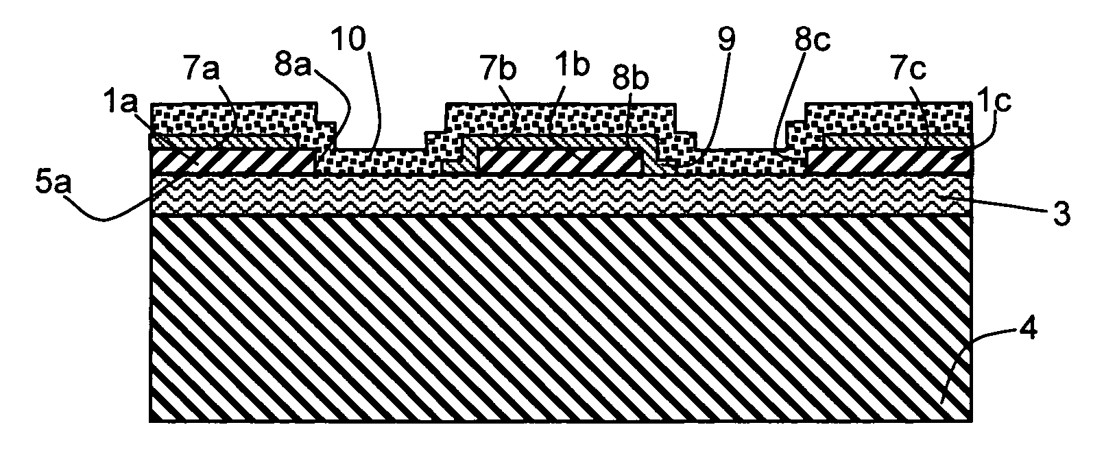
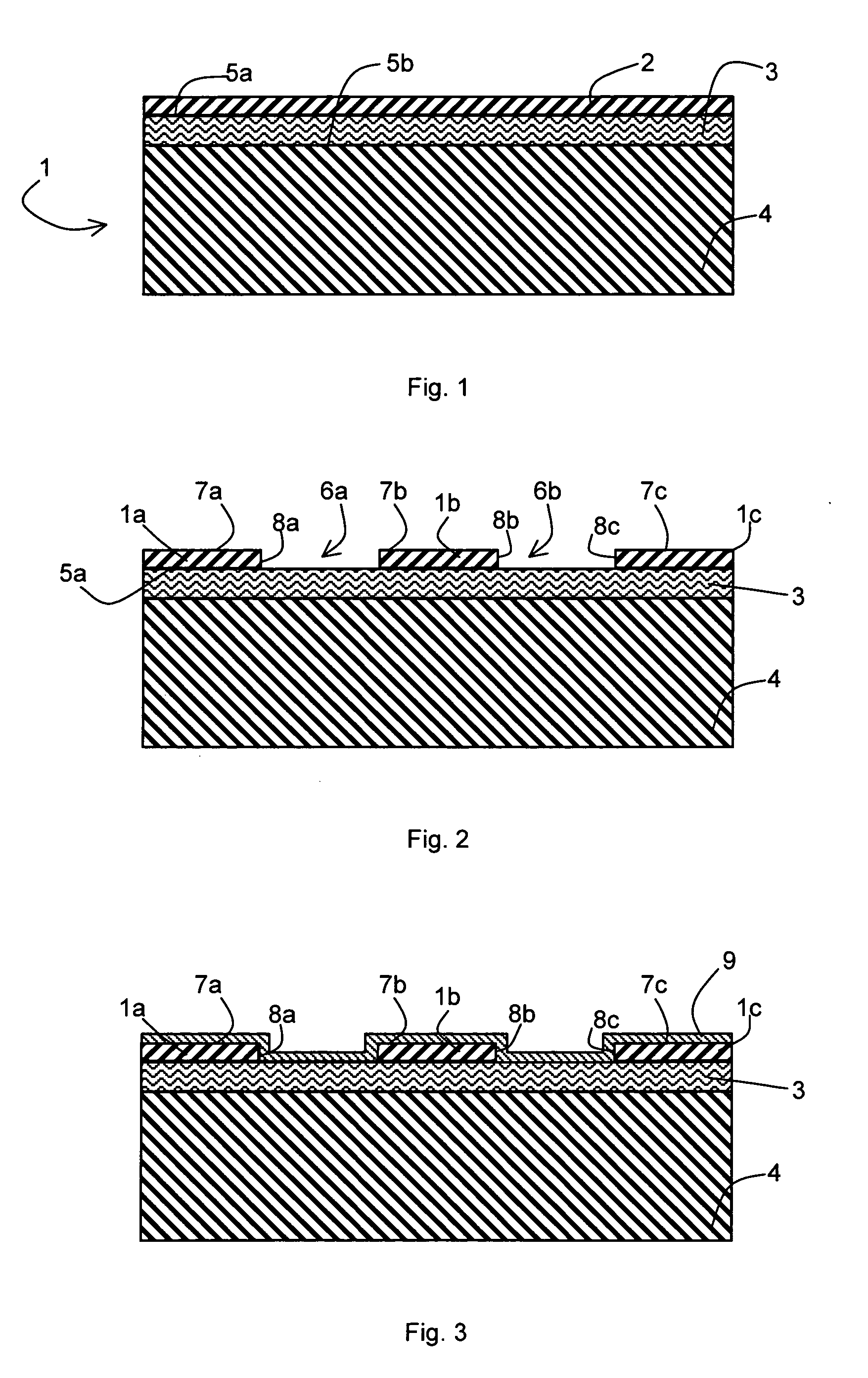
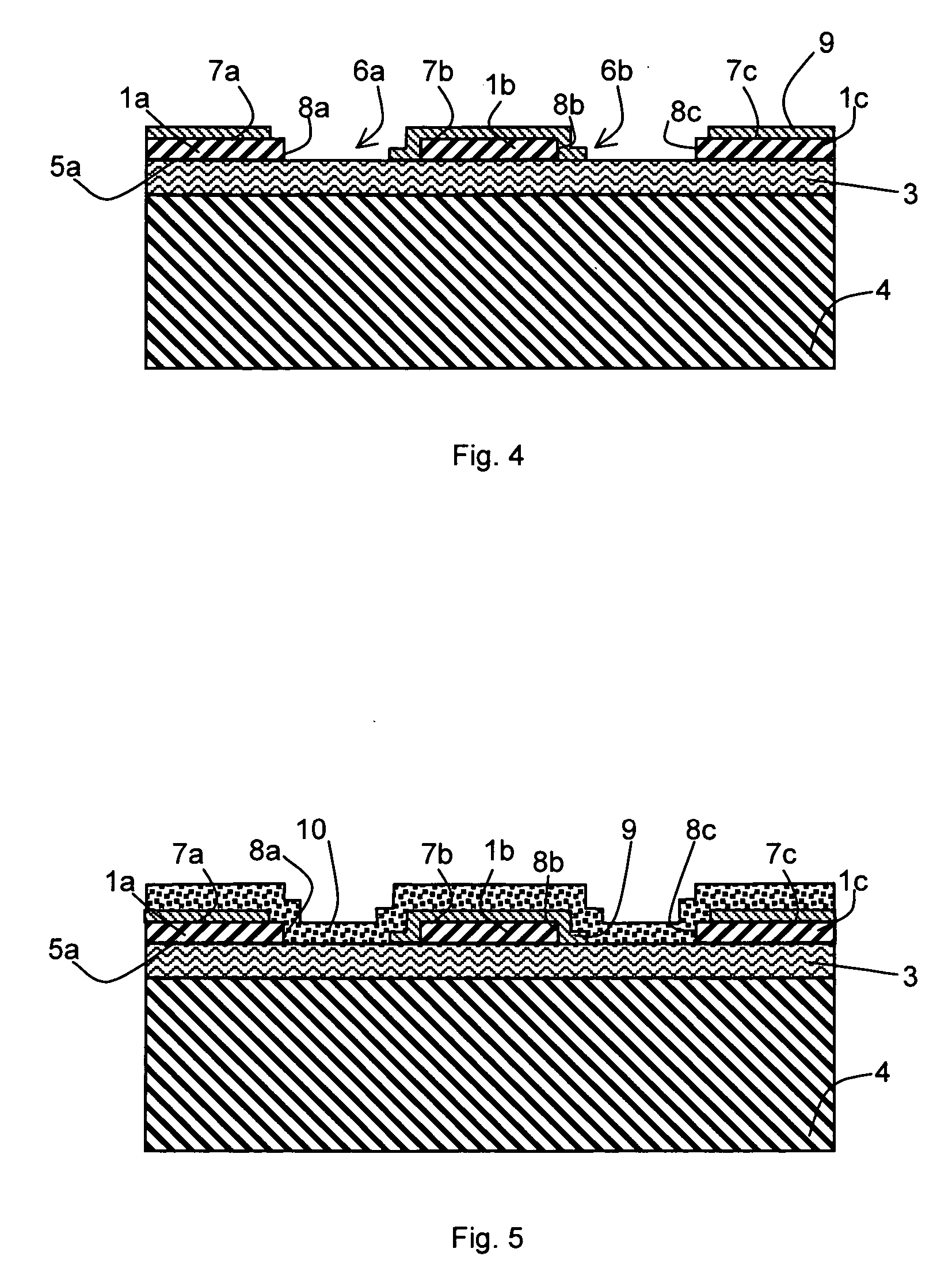
[0016] A method according to the invention enables first and second active zones, respectively formed by distinct first and second monocrystalline semi-conducting materials, to be achieved simply and inexpensively on the front face of a support. In addition, it enables the front faces of the first and second active zones to be in the same plane as one another, and the first and second semi-conducting materials preferably have identical crystalline structures.
[0017] Such a method consists in particular in producing the second active zones by a crystallization step of the second semi-conducting material in monocrystalline form from patterns made of second semi-conducting material in polycrystalline and / or amorphous form and from interface regions between said patterns and preselected first active zones.
[0018] According to a particular embodiment, the crystallization step is preferably performed by a localized solidification method. In this case, the second semi-conducting material h...
PUM
 Abstract
Description
Claims
Application Information