CMOS transistor junction regions formed by a CVD etching and deposition sequence

a transistor junction and etching technology, applied in the field of cmos transistors, can solve the problems of limiting the current flow from the channel to salicide contact, the shape of the recess, and the inability to fully optimize the spreading resistan

Active Publication Date: 2007-05-10
DAEDALUS PRIME LLC
View PDF9 Cites 29 Cited by
  • Summary
  • Abstract
  • Description
  • Claims
  • Application Information

AI Technical Summary

Problems solved by technology

This narrow band of dopants leads to high spreading resistance, and limits the current flow from channel to salicide contact.
In state of the art replacement source-drain architectures, the shape of the recess is better, but is still not fully optimized with respect to spreading resistance.

Method used


Image

  • CMOS transistor junction regions formed by a CVD etching and deposition sequence
  • CMOS transistor junction regions formed by a CVD etching and deposition sequence
  • CMOS transistor junction regions formed by a CVD etching and deposition sequence

Examples


Embodiment Construction

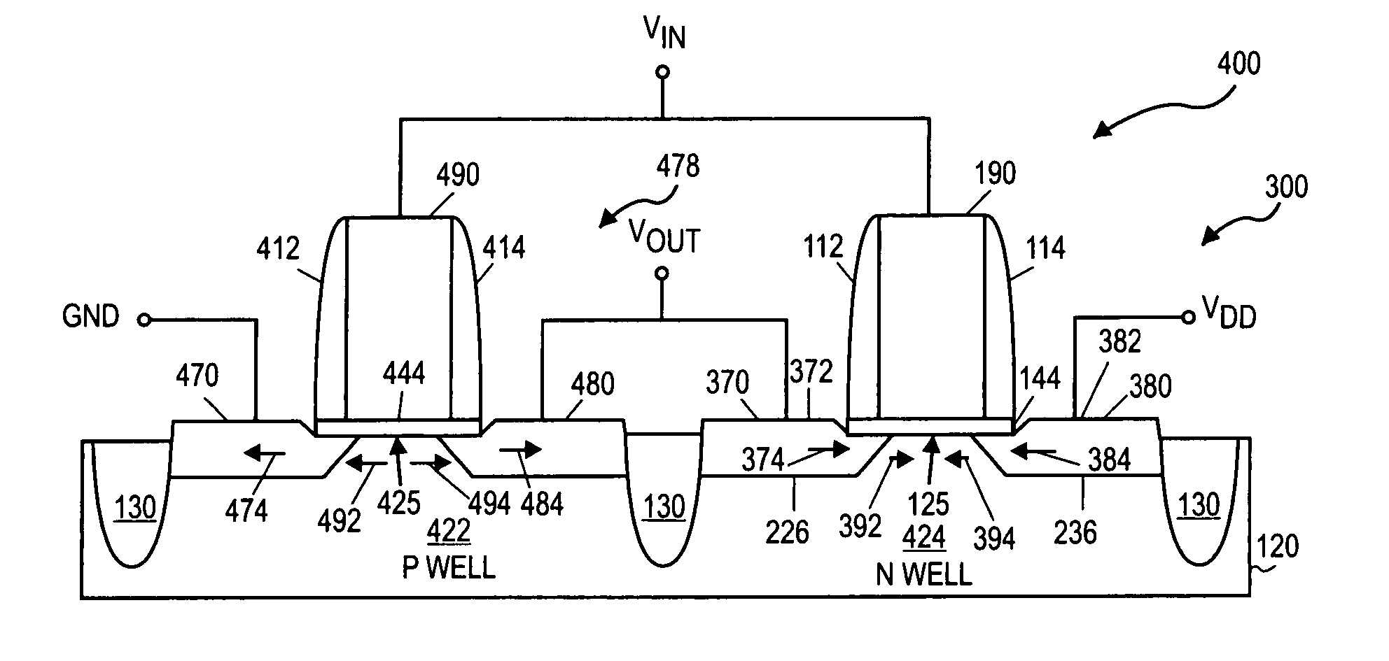
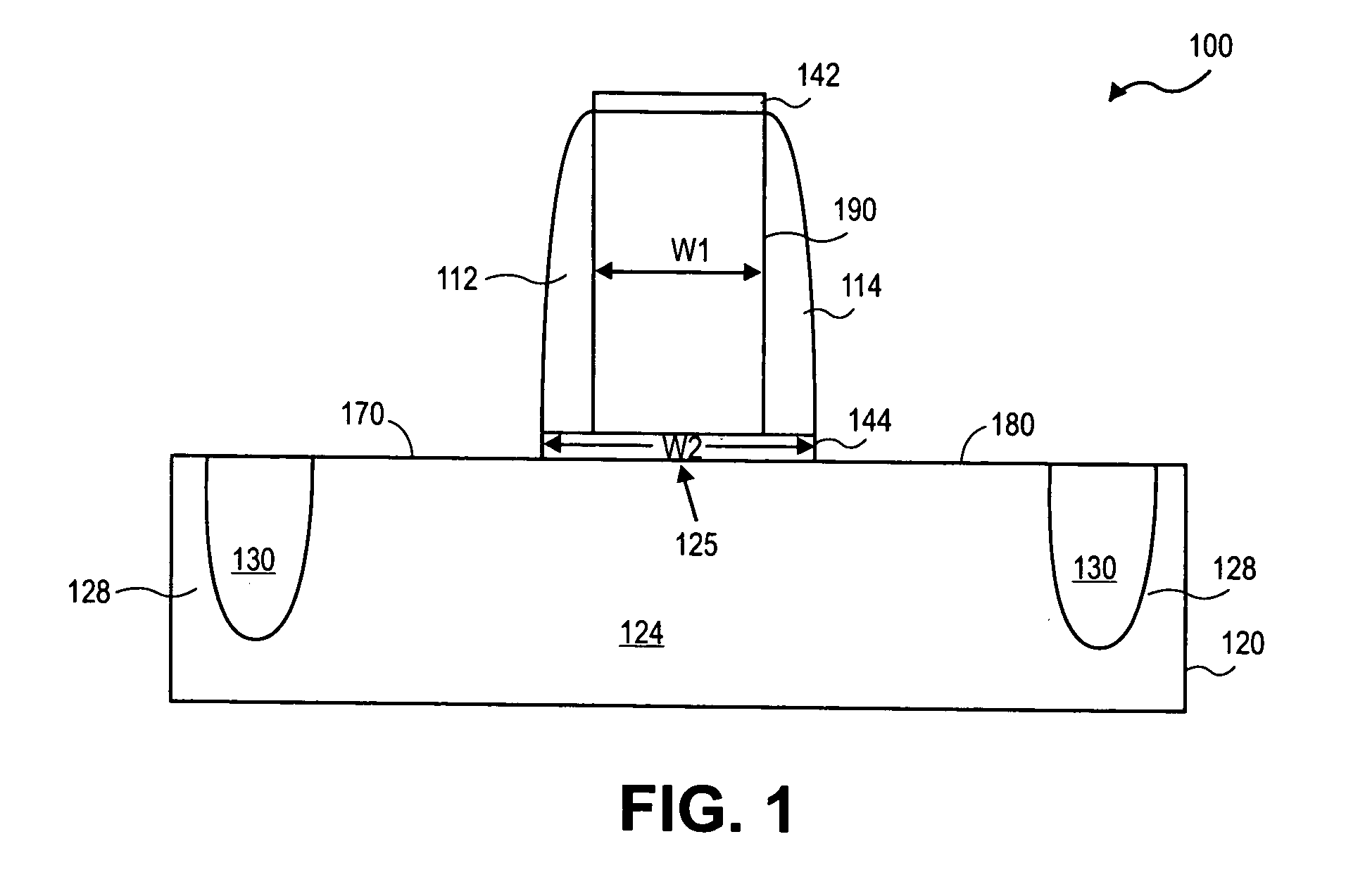
[0020] Locally straining transistor channel regions may be accomplished by selective epitaxial deposition of source and drain regions with materials that impart a strain in a MOS transistor's channel region. Such process flows may involve etching the substrate material from the source-drain regions of the transistor in one process operation using an etch reactor. A subsequent operation may involve replacing the removed material with Si alloy material in a deposition reactor. The etch reactor and deposition reactor may be physically different and separate. Thus the substrate must be removed from the etch reactor and exposed to atmospheric pressure environments before initiating the Si alloy deposition process. The Si alloy may be pure Si or Si1-xGex or Si1-xCx and can be undoped or doped with p-type or n-type dopants. The deposition process may be selective or non-selective. According to embodiments provided herein, the etch reactor and deposition reactor may be physically the same. ...


PUM


Abstract

This invention adds to the art of replacement source-drain cMOS transistors. Processes may involve etching a recess in the substrate material using one equipment set, then performing deposition in another. Disclosed is a method to perform the etch and subsequent deposition in the same reactor without atmospheric exposure. In-situ etching of the source-drain recess for replacement source-drain applications provides several advantages over state of the art ex-situ etching. Transistor drive current is improved by: (1) Eliminating contamination of the silicon-epilayer interface when the as-etched surface is exposed to atmosphere and (2) Precise control over the shape of the etch recess. Deposition may be done by a variety of techniques including selective and non-selective methods. In the case of blanket deposition, a measure to avoid amorphous deposition in performance critical regions is also presented.

Description

CROSS REFERENCE TO RELATED CASES [0001] This patent application is a divisional of U.S. patent application Ser. No. 11 / 029,740 filed Jan. 4, 2005 entitled, “CMOS Transistor Junction Regions Formed by a CVD Etching and Deposition Sequence.”BACKGROUND [0002] Circuit devices and the manufacture and structure of circuit devices. Background [0003] Increased performance in circuit devices on a substrate (e.g., integrated circuit (IC) transistors, resistors, capacitors, etc. on a semiconductor (e.g., silicon) substrate) is typically a major factor considered during design, manufacture, and operation of those devices. For example, during design and manufacture or forming of metal oxide semiconductor (MOS) transistor devices, such as those used in a complementary metal oxide semiconductor (CMOS), it is often desired to increase movement of electrons in N-type MOS device (n-MOS) channels and to increase movement of positive charged holes in P-type MOS device (p-MOS) channels. A key parameter ...

Claims


Application Information

Patent Timeline
Patent Type & Authority Applications(United States)
IPC IPC(8): H01L21/331
CPCH01L21/02381H01L21/02532H01L21/0262H01L21/02639H01L29/517H01L29/66628H01L29/7834H01L29/7848H01L21/2053H01L21/8238B82Y40/00H01L21/18H01L21/205H01L21/3065
Inventor MURTHY, ANANDGLASS, GLENN A.WESTMEYER, ANDREW N.HATTENDORF, MICHAEL L.WANK, JEFFREY R.
Owner DAEDALUS PRIME LLC
Why Eureka
Try Eureka