Method of fabricating a microelectronic device using electron beam treatment to induce stress

a microelectronic device and electron beam technology, applied in semiconductor/solid-state device manufacturing, basic electric elements, electric apparatus, etc., can solve problems such as limiting scalability and device performance, limiting channel mobility, and limiting the benefits obtained from the use of such liners, which have begun to encounter process limitations

Inactive Publication Date: 2007-05-10
TEXAS INSTR INC
View PDF6 Cites 14 Cited by
  • Summary
  • Abstract
  • Description
  • Claims
  • Application Information

AI Technical Summary

Problems solved by technology

One characteristic that limits scalability and device performance is electron and hole mobility, also referred to as channel mobility, throughout the channel region of transistors.
As devices continue to shrink in size, the channel region for transistors continues to also shrink in size, which can limit channel mobility.
However, due to advances in technologies, the benefits obtained from the use of such liners as begun to encounter process limitations.
Unfortunately, however, the amount of stress that can be incorporated into

Method used


Image

  • Method of fabricating a microelectronic device using electron beam treatment to induce stress
  • Method of fabricating a microelectronic device using electron beam treatment to induce stress
  • Method of fabricating a microelectronic device using electron beam treatment to induce stress

Examples


Embodiment Construction

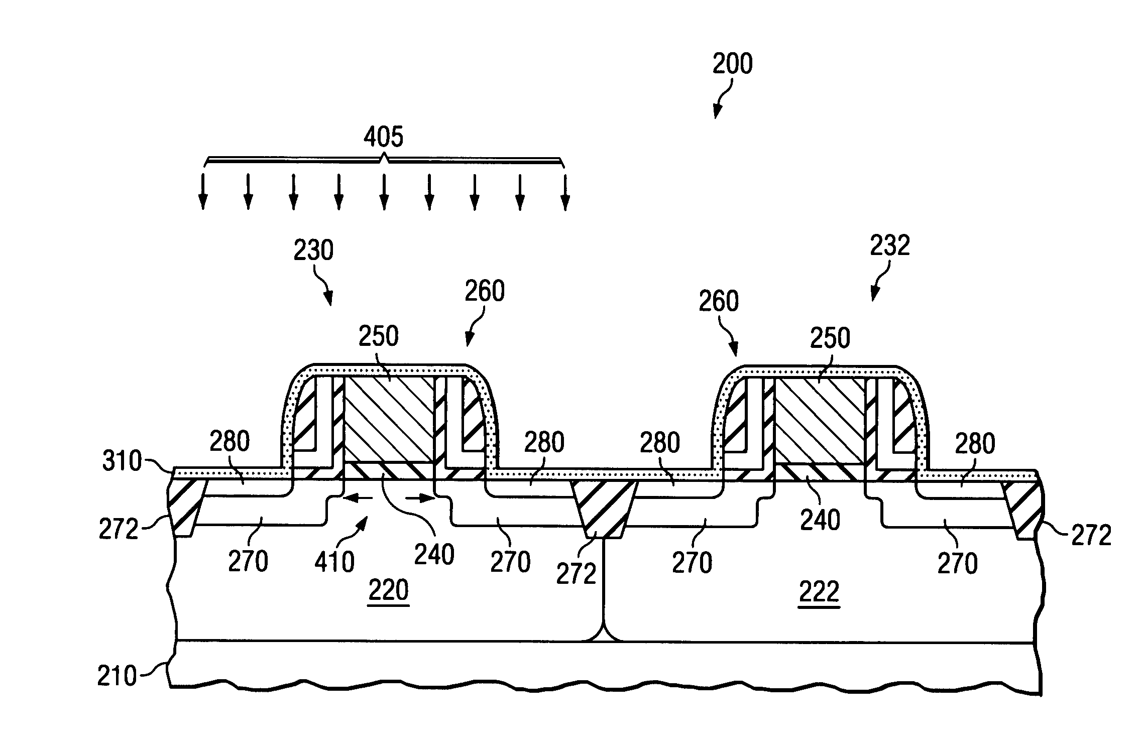
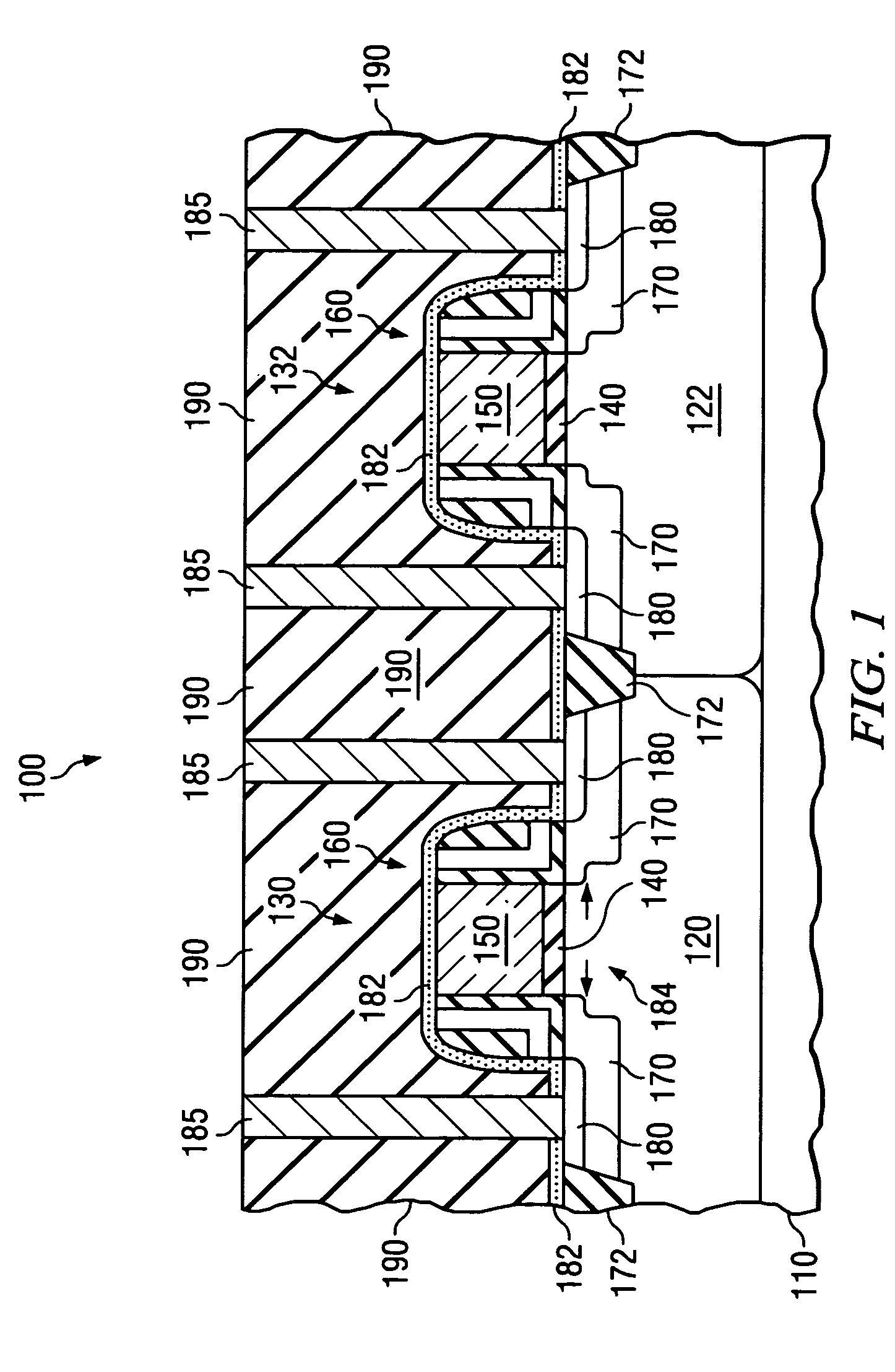
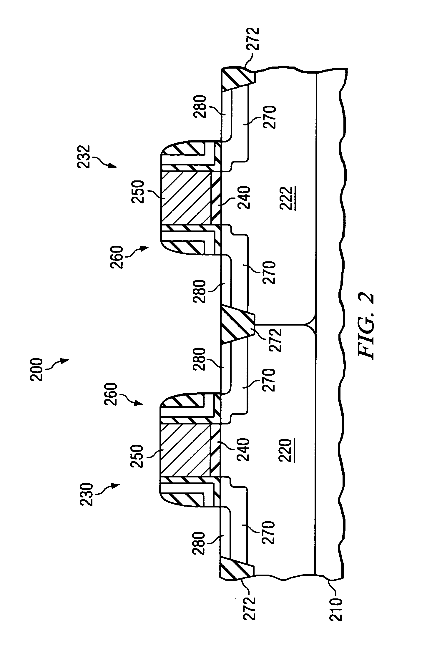
[0018] Turning initially to FIG. 1, there is illustrated a partial sectional view of one embodiment of a microelectronics device 100, as provided by the present invention. The microelectronics device 100 includes a conventional semiconductive substrate 110, such as appropriately doped silicon. Other semiconductive materials well known to those skilled in the art may also be used. Located within the substrate 110 in the embodiment of FIG. 1 are complementary doped well regions 120 and 122. Located over the substrate 110 and well regions 120 and 122, respectively, is an NMOS gate structure 130 and a PMOS gate structure 132. In this particular embodiment, the gate structures 130, 132 are complementary NMOS and PMOS devices, with the NMOS device being located over the well region 120 and the PMOS device being located over the well region 122. However, it should be understood that the present invention is not limited to a particular device configuration. For example, in certain embodimen...


PUM


Abstract

The present invention, in one embodiment, provides a method of fabricating a microelectronics device 200. This embodiment comprises forming a liner 310 over a substrate 210 and a gate structure 230, subjecting the liner 310 to an electron beam 405 and depositing a pre-metal dielectric layer 415 over the liner 310.

Description

TECHNICAL FIELD OF THE INVENTION [0001] The present invention is directed in general to a method for manufacturing a microelectronics device, and more specifically, to a method of inducing stress into a channel region of a microelectronics device. BACKGROUND [0002] There exists a continuing need to improve semiconductor device performance and further scale microelectronic devices. One characteristic that limits scalability and device performance is electron and hole mobility, also referred to as channel mobility, throughout the channel region of transistors. As devices continue to shrink in size, the channel region for transistors continues to also shrink in size, which can limit channel mobility. [0003] One technique that may improve scaling limits and device performance is to introduce strain into the channel region, which can improve electron and hole mobility. Different types of strain, including expansive strain, tensile strain, and compressive strain, have been introduced into...

Claims


Application Information

Patent Timeline
IPC IPC(8): H01L21/469
CPCH01L21/3105H01L21/3148H01L21/3185H01L21/823807H01L21/823864H01L21/02167H01L21/0217
Inventor TSUI, TING Y.MCKERROW, ANDREWBU, HAOWENKRAFT, ROBERT
Owner TEXAS INSTR INC
Why Eureka
Try Eureka