
Integrated Circuit Having a Multipurpose Resistor for Suppression of a Parasitic Transistor or Other Purposes

a multi-purpose resistor and integrated circuit technology, applied in the direction of diodes, semiconductor devices, electrical apparatus, etc., can solve the problems of composite ldmosfet circuits that have not been properly operated, terminals coupled to drain regions of one device gain negative potentials, and parasitic transistors that have so far been prone to conduction, etc., to achieve convenient use and more reliable operation

Active Publication Date: 2007-05-17
SANKEN ELECTRIC CO LTD
View PDF3 Cites 23 Cited by
  • Summary
  • Abstract
  • Description
  • Claims
  • Application Information

AI Technical Summary

Benefits of technology

[0010] The present invention has it as a general object to make integrated circuits of the kind under consideration more reliable in operation and convenient of use.
[0012] Another specific object of the invention is to enhance the utility of integrated circuits of the kind in question in their intended applications to startup circuits or current detector circuits.
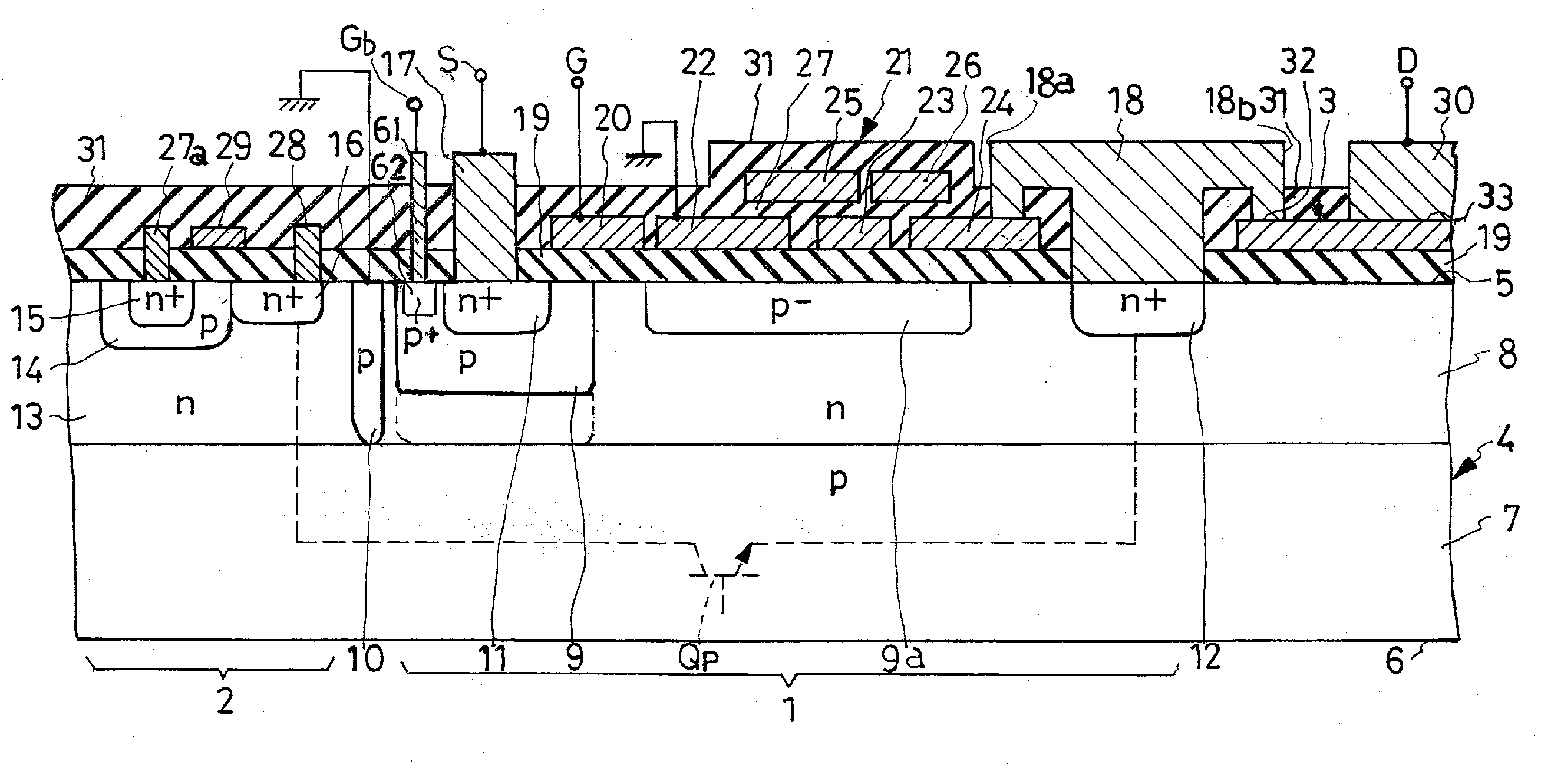
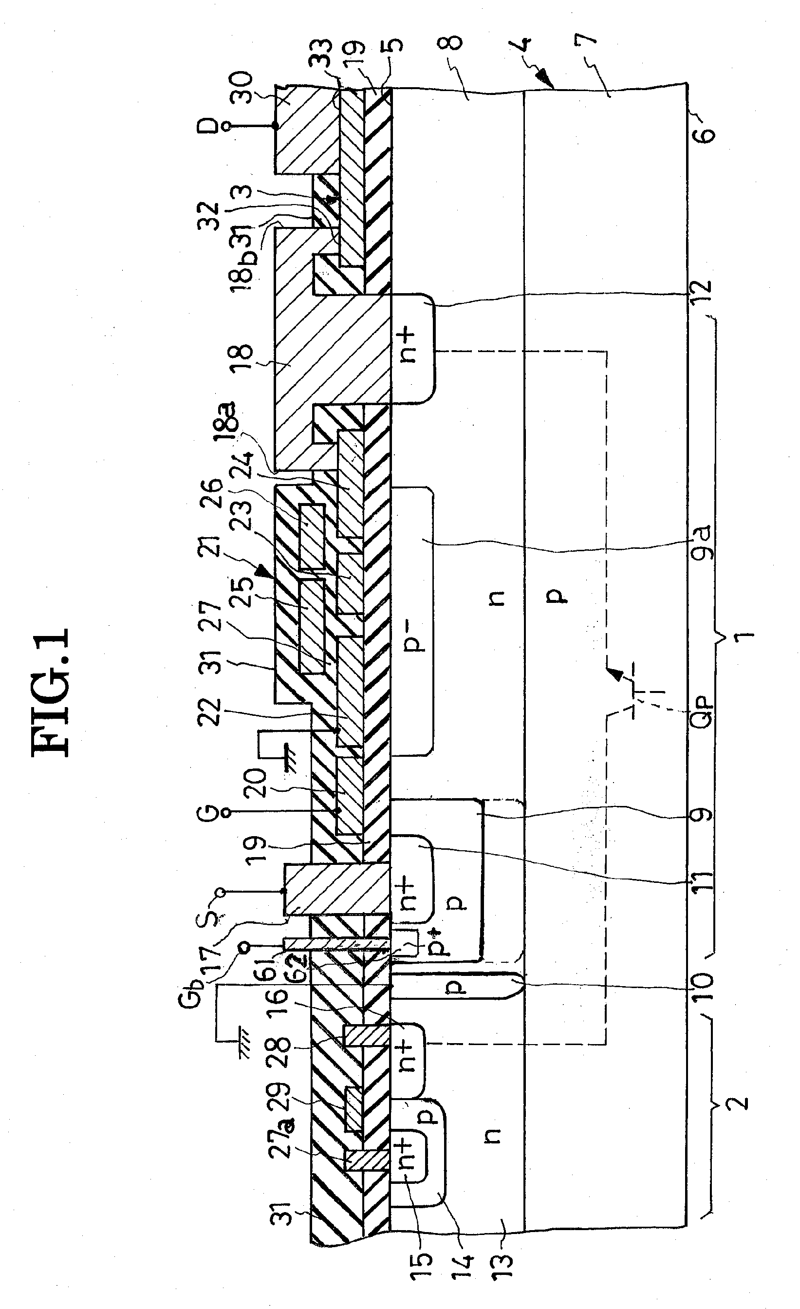
[0014] The multipurpose resistor or diode, being coupled to the second electrode as above, limits the magnitude of the current flowing between the first and the second electrode. In some applications of the invention in which a capacitor is connected between the first electrode and the ground, the multipurpose resistor or diode is capable of restricting the flow of rush current into the capacitor.
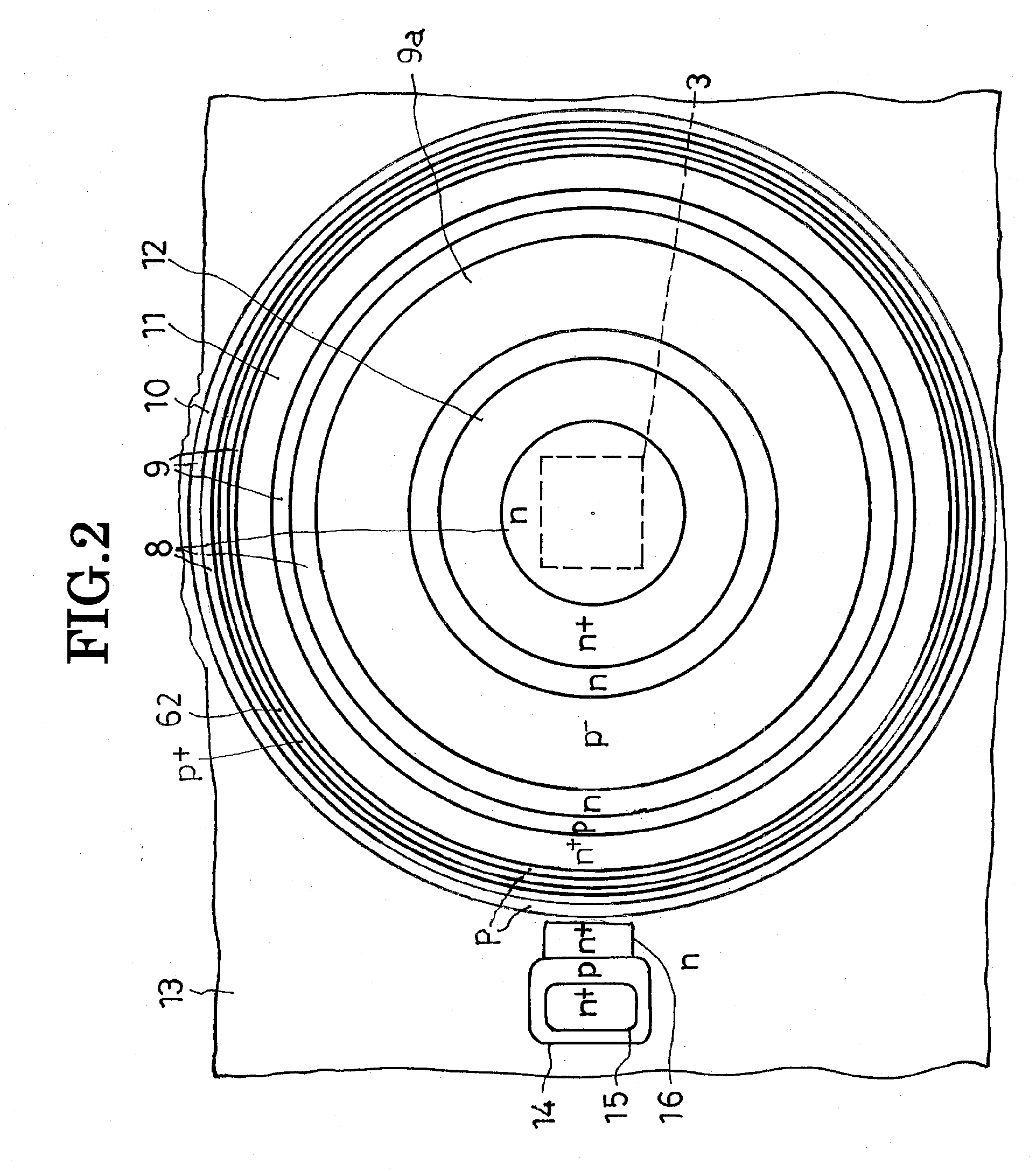
[0015] A representative embodiment of the invention takes the form of a composite integrated circuit incorporating a first and a second semiconductor device of unlike configurations, with a separator region therebetween for electrically isolating them from each other. The multipurpose resistor or diode according to the invention serves to prevent the conduction of the parasitic transistor that appears of necessity in this type of integrated circuit.
[0017] It will be appreciated in particular that the multipurpose resistor or diode is an integral part of the integrated circuit, being formed directly on the substrate via an insulating layer. This offers an additional advantage in applications where a semiconductor device or devices that are capable of fabrication in the form of the integrated circuit according to the invention are put to use in combination with a discrete resistor or diode comparable to the multipurpose resistor or diode of this invention. Constituting an integral part of the integrated circuit, the multipurpose resistor or diode according to the invention replaces the conventional discrete resistor or diode, saving space or area for their installation.
[0018] A further embodiment is disclosed in which the integrated two semiconductor devices are isolated from each other by two separator regions of the same conductivity type and an anti-parasitic-transistor region of the opposite conductivity type interposed between the separator regions. The provision of this anti-parasitic-transistor region results in the creation of a second parasitic transistor, in addition to the first which is inherent in this type of composite integrated circuit. The second parasitic transistor is so configured that it will turn on upon accidental application to the second electrode of a voltage of a polarity capable of causing conduction therethrough. The first parasitic transistor will be left inactivated upon conduction of the second. Thus the first parasitic transistor is dually prevented from conduction in this embodiment, both by the multipurpose resistor or diode and by the anti-parasitic-transistor region between the two separator regions.

Problems solved by technology

They share the p-type substrate region, however, so that the composite LDMOSFET circuit gives rise to a parasitic npn transistor composed of that p-type substrate region and the n-type drain regions of the two devices.
This parasitic transistor has so far been prone to conduction as when the drain terminal coupled to the drain region of one device gains a negative potential due for example to noise.
Then, of course, the composite LDMOSFET circuit has not operated correctly.
The same problem has manifested itself when two bipolar transistors, rather than LDMOSFETs, are integrated in a like manner, too.
This solution is objectionable for the additional manufacturing steps required for creation of the n−-type substrate region.
The provision of the discrete anti-parasitic-transistor circuit makes the combination of this circuit and the composite LDMOSFET circuit difficult of manufacture and handling and adds to its installation space or area requirement.
The integrated composite LDMOSFET circuit has had an additional problem in its important application to a switching-mode power supply.

Method used


Image

  • Integrated Circuit Having a Multipurpose Resistor for Suppression of a Parasitic Transistor or Other Purposes
  • Integrated Circuit Having a Multipurpose Resistor for Suppression of a Parasitic Transistor or Other Purposes
  • Integrated Circuit Having a Multipurpose Resistor for Suppression of a Parasitic Transistor or Other Purposes

Examples


embodiment

of FIG. 5

[0085] Shown fragmentarily in FIG. 5 is the second preferred form of composite integrated circuit which features an annular trench 10a, complete with a filling 60 of electrically insulating material, in place of the separator region 10, FIGS. 1 and 2. All the other details of construction are as previously set forth in connection with FIGS. 1-3.

[0086] The trench 10a. extends from the top surface 5 of the substrate 4 down to the first semiconductor region 7. Filled with the insulator 60, the trench 10a electrically separates the first and the second semiconductor device 1 and 2 from each other. The trench 10a could be disposed contiguous to the third substrate region 9 or body region of the first semiconductor device 1. The terminal Gb extending from the electrode 61 may be connected as required to the source terminal S.

[0087] It is understood that the composite integrated circuit of FIG. 5 incorporates an multipurpose resistor similar to that seen at 3 in FIGS. 1-3 and so...


PUM


Abstract

A composite integrated circuit incorporating two LDMOSFETs of unlike designs, with the consequent creation of a parasitic transistor. A multipurpose resistor is integrally built into the composite integrated circuit in order to prevent the parasitic transistor from accidentally turning on. In an intended application of the composite integrated circuit to a startup circuit of a switching-mode power supply, the multipurpose resistor serves as startup resistor for limiting the flow of rush current during the startup period of the switching-mode power supply.

Description

CROSS REFERENCE TO RELATED APPLICATIONS [0001] This application claims priority to Japanese Patent Application No. 2005-327677, filed Nov. 11, 2005. BACKGROUND OF THE INVENTION [0002] This invention relates to integrated circuits, to monolithic integrated circuits of semiconductor devices as well as passive components, and particularly to a composite integrated circuit incorporating two or more semiconductor devices of like or unlike constructions, possibly with consequent creation of a parasitic transistor. More particularly, the invention deals with such an integrated circuit featuring provisions for preventing the conduction of the parasitic transistor, limiting current flow, or other purposes. [0003] It has been known to integrate two or more semiconductor devices into a single microchip, with the integrated devices electrically separated from each other either by pn junction isolation or a combination of pn junction and trench isolations, as disclosed for example in Japanese Un...

Claims


Application Information

Patent Timeline
IPC IPC(8): H01L29/76
CPCH01L27/0629H01L29/0634H01L29/404H01L29/7817
Inventor SEKIGUCHI, KEIICHIAIZAWA, KAZUYA
Owner SANKEN ELECTRIC CO LTD
Learn More