Integrated circuit comprising a gradually doped bipolar transistor and corresponding fabrication process

a technology of integrated circuits and bipolar transistors, which is applied in the direction of basic electric elements, semiconductor devices, electrical equipment, etc., can solve the problems of imposing excessive alignment constraints during photolithography steps, difficult to produce a conventionally doped collector, and process incurring a cost increase in fabricating an integrated circui

Active Publication Date: 2007-05-17
STMICROELECTRONICS SRL
View PDF5 Cites 6 Cited by
  • Summary
  • Abstract
  • Description
  • Claims
  • Application Information

AI Technical Summary

Benefits of technology

[0012] Preferably, the substrate used is a silicon-on-insulator (SOI) substrate, thereby making it possible for the dopant species to be made electrically inactive in the central zone of the substrate more effectively.
[0013] Advantageously, the collector of the transistor may be self-aligned with the base / emitter window, thereby making it possible to obtain a reproducible concentration profile of dopant species.

Problems solved by technology

However, producing such an architecture has the drawback of using additional masks so as to localize, beneath the base of the transistor, the zone of the collector region that it is desired to dope laterally in a gradual manner.
Thus, such a process has the drawback of imposing excessively severe alignment constraints during the photolithography steps.
Furthermore, the transition frequencies and the breakdown voltage of a transistor vary according to the misalignment of the masks used during this process, making it particularly difficult to produce a gradually doped collector in a conventional manner.
Such a process also incurs a cost increase in fabricating an integrated circuit, due to the use of additional masks.

Method used


Image

  • Integrated circuit comprising a gradually doped bipolar transistor and corresponding fabrication process
  • Integrated circuit comprising a gradually doped bipolar transistor and corresponding fabrication process
  • Integrated circuit comprising a gradually doped bipolar transistor and corresponding fabrication process

Examples


Embodiment Construction

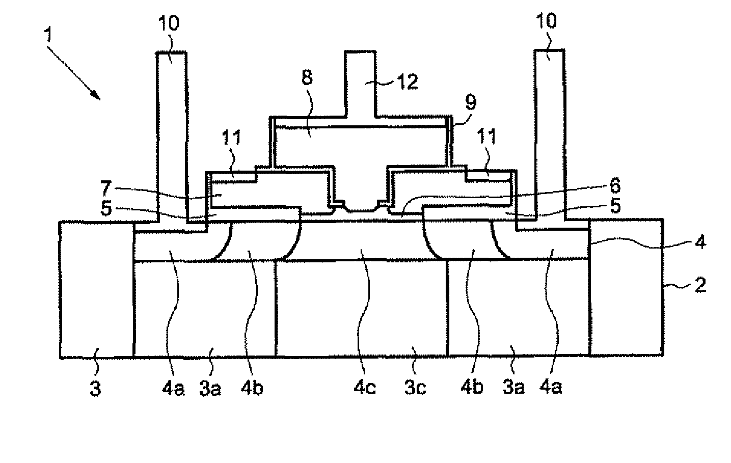
[0020] Illustrated in FIG. 1 is a bipolar transistor 1 of an integrated circuit comprising a substrate 2, which may be a silicon-on-insulator (SOI) substrate. The substrate 2 has a lower portion 3 comprising the insulator, partly surmounted by a layer 4 forming a collector which may be made of n-doped silicon, for example using arsenic or phosphorus.

[0021] The bipolar transistor 1 also includes on the upper surface of the collector 4 insulation layers 5 spaced apart by a layer 6 of SixGe1-xCy having a percentage germanium content of generally between 10% and 40% and a percentage carbon content substantially less than 1%, for example around 0.05%. In other words, the insulator layers 5 cover the upper surface of the collector 4 so as to leave, in the middle of the surface, a window for the SixGe1-xCy layer 6. The thickness of the layer 6 is typically from 50 to 70 nm.

[0022] The insulator layers 5 may have ends that extend vertically so as to form a well that partly supports thick l...


PUM


Abstract

An integrated circuit includes a bipolar transistor comprising a substrate and a collector formed in the substrate. The collector includes a highly doped lateral zone, a very lightly doped central zone and a lightly doped intermediate zone located between the central zone and the lateral zone 4a of the collector. The substrate includes a lightly doped lateral zone and a highly doped central zone. The dopant species in the zone of the substrate are electrically inactive.

Description

FIELD OF THE INVENTION [0001] The present invention relates to integrated circuits, and more particularly, to laterally operating bipolar transistors comprising a gradually doped collector region. BACKGROUND OF THE INVENTION [0002] The production of bipolar transistors assembled with standard CMOS transistors within a semiconductor substrate or a silicon-on-insulator (SOI) substrate makes it possible at the present time to obtain integrated circuits of high electrical performance. Bipolar transistor architectures are preferably characterized at the present time by a double emitter / base / collector heterojunction of the polysilicon / carbon-containing SiGe alloy / silicon type. Bipolar transistors having such architectures may be used in the high-frequency field, especially for frequencies above 50 GHz. [0003] The electrical performance of bipolar transistors is generally determined from the measurement of the transition frequency of the transistor as a function of the breakdown voltage of...

Claims


Application Information

Patent Timeline
Patent Type & Authority Applications(United States)
IPC IPC(8): H01L31/11
CPCH01L29/0821H01L29/66242H01L29/7317H01L29/7378
Inventor LENOBLE, DAMIENSCHWARTZMANN, THIERRYBOISSONNET, LAURENCE
Owner STMICROELECTRONICS SRL
Why Eureka
Try Eureka