Drive element mount display

a technology of mounting brackets and elements, applied in semiconductor devices, semiconductor/solid-state device details, instruments, etc., can solve problems such as narrowing down the frame area, and achieve the effects of preventing the cost increase of the driver, reducing the load, and minimizing the cost increase of the semiconductor substra

Inactive Publication Date: 2007-05-17
SHARP KK
View PDF18 Cites 22 Cited by
  • Summary
  • Abstract
  • Description
  • Claims
  • Application Information

AI Technical Summary

Benefits of technology

[0013] According to the arrangement, for example, even when a liquid crystal driver with a large number of outputs of fine pitches is mounted, there is no need to match the pitches of the terminals of the signal wires of the display means to the fine pitches of the liquid crystal driver. In addition, the driver can be made with fine pitches without considering the pitches of the terminals of the signal wires of the display means. The arrangement therefore limits increases of wiring regions where the group of input / output terminals of the driver are connected to the terminals of the signal wires of the display means even in COG mounting where the drive element is mounted onto the frame of the transparent substrate of the display means. Thus, the driver with a large number of outputs of fine pitches can be mounted onto the transparent substrate without adding to the frame area.
[0030] If a signal wire of the display means is cut off in the middle, the cut-off line does not properly turn on. To prevent this from happening, a solution is known which saves by feeding drive signals from the other end of the cut-off line. The solution adds to the load due to the connection of signal lines and other factors, requiring drive buffers with larger-than-usual driving capability. The mounting of the large redundant buffers to the driver which is fabricated by a fine process is costly. Accordingly, in the arrangement, the redundant buffer elements are mounted to the semiconductor substrate. The structure minimizes cost increase of the semiconductor substrate manufactured by a non-fine, old generation semiconductor process, while still preventing cost increase of the driver.

Problems solved by technology

However, fine output wire pitches in liquid crystal drivers raise the following problems.
This could be an obstacle in narrowing down the frame area. FIG. 16 shows how the output pitch of the liquid crystal driver can affect a wiring region of the liquid crystal panel.

Method used


Image

  • Drive element mount display
  • Drive element mount display
  • Drive element mount display

Examples


embodiment 1

[0049] An embodiment of the liquid crystal driver mount display in accordance with the present invention will be described. The following description contains various limitations that are preferable from a technical point of view to implement the present invention. The present invention is however by no means limited by the embodiments and figures.

[0050] Referring to FIG. 1 to FIG. 4, the following will describe the liquid crystal driver mount display in accordance with the present invention.

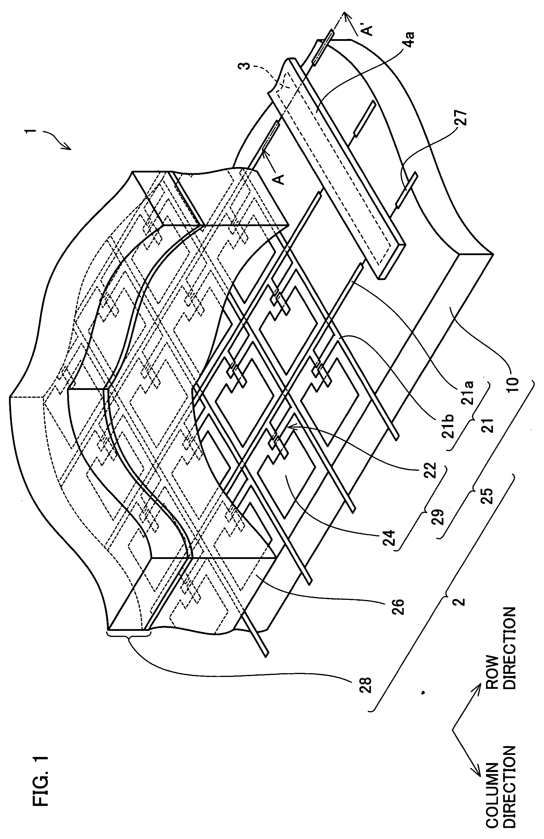
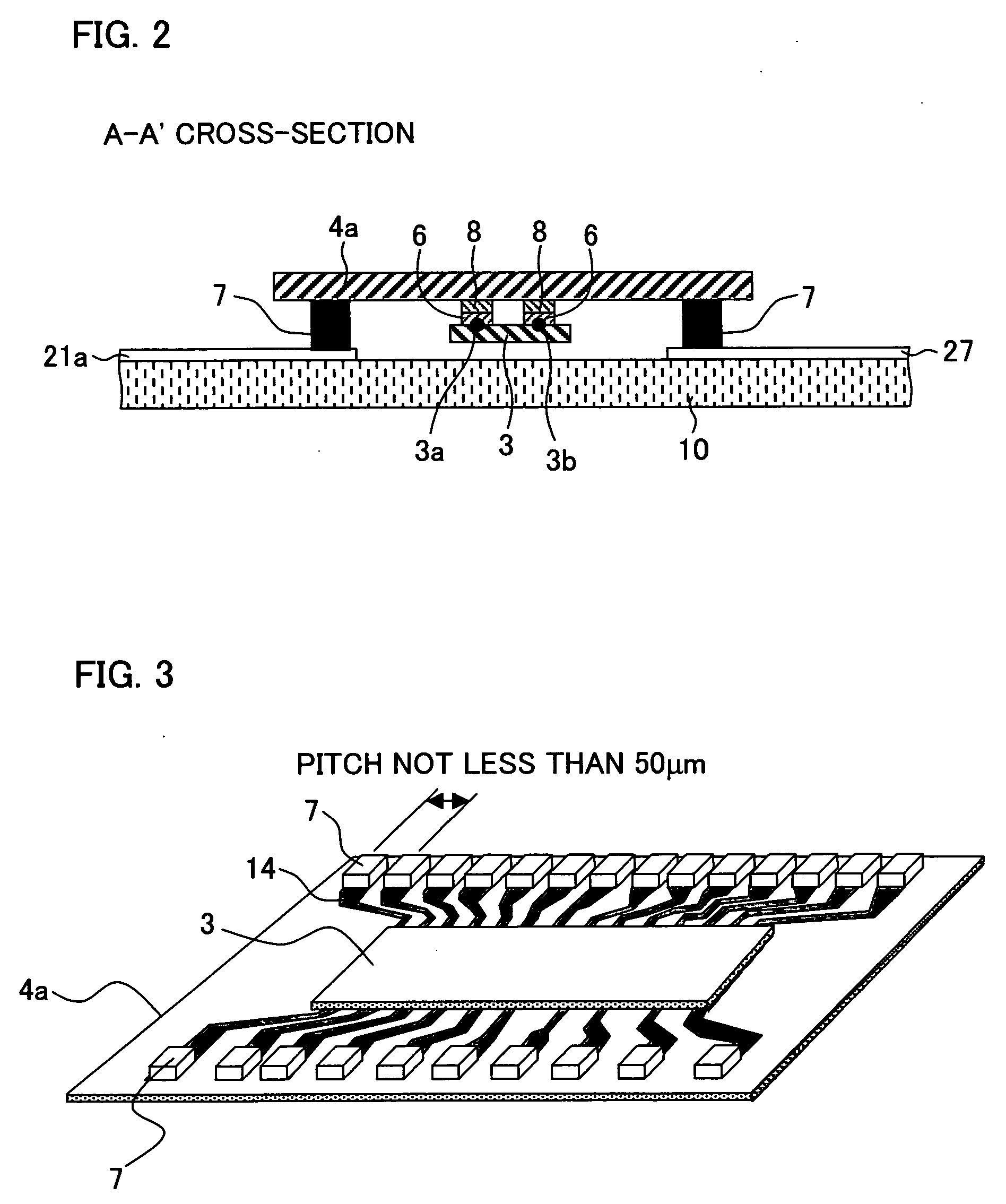
[0051]FIG. 1 is an oblique view showing the structure of a liquid crystal driver mount display which is an embodiment of the present invention. The liquid crystal driver mount display 1 of the present embodiment includes, as shown in FIG. 1, a liquid crystal display means (display means, liquid crystal display body) 2, a liquid crystal driver (driver) 3, and a driver socket (semiconductor substrate) 4a.

[0052] The liquid crystal display means 2 includes an active matrix substrate 25, a liquid ...

embodiment 2

[0075] The following will describe another embodiment of the present invention in reference to FIG. 5. The embodiment will focus on differences from embodiment 1. For convenience, members of the present embodiment that have the same arrangement and function as members of embodiment 1, and that are mentioned in that embodiment are indicated by the same reference numerals and description thereof is omitted.

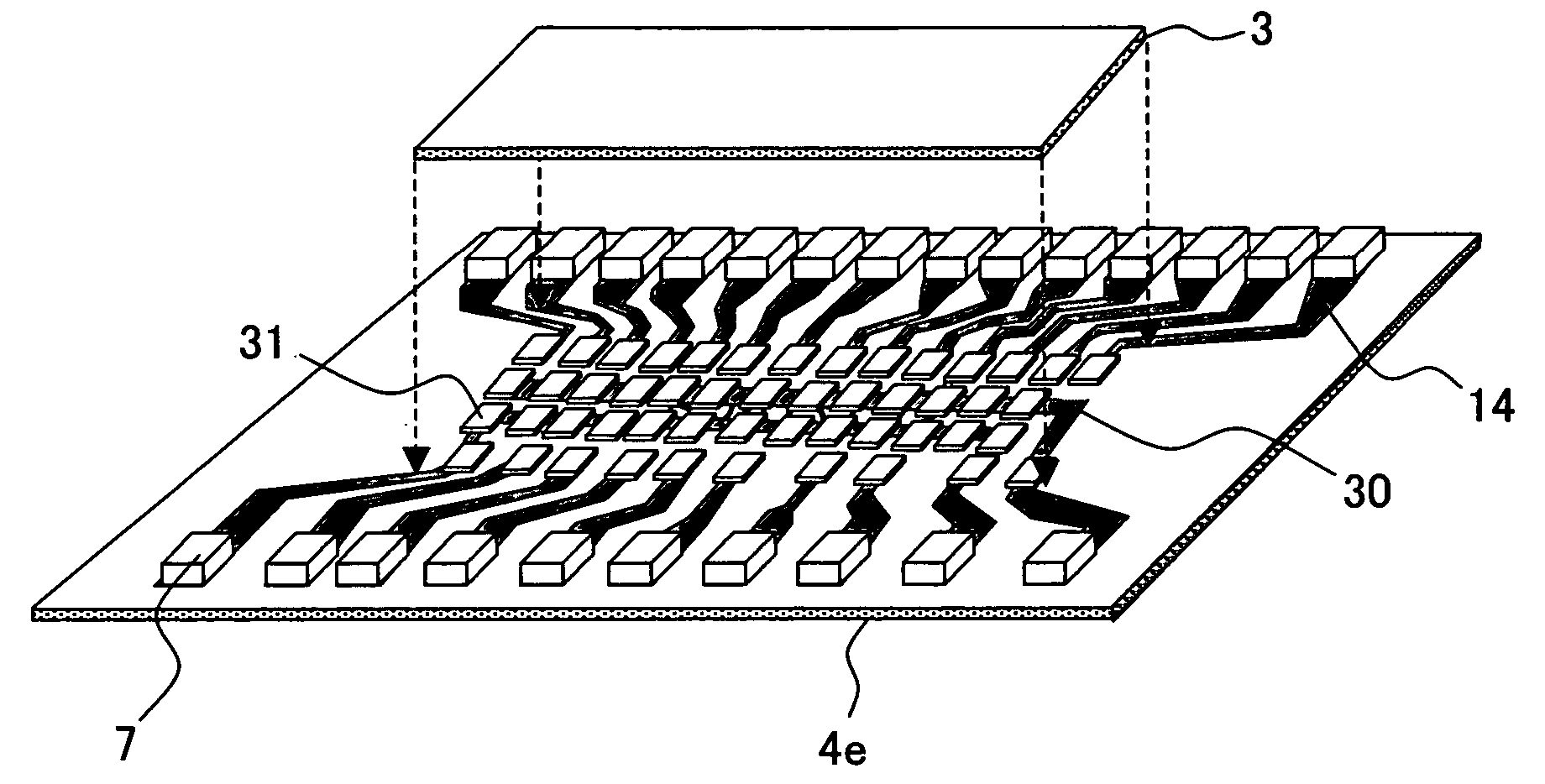
[0076]FIG. 5 is an oblique view showing the structure of a driver socket 4b of the liquid crystal driver mount display 1 of the present embodiment. The driver socket 4b of the liquid crystal driver mount display 1 shown in FIG. 5 includes a driver socket 4b in place of the driver socket 4a of the liquid crystal driver mount display 1 described in embodiment 1. The driver socket 4b has metal wires 14′ of a multilayer structure on the socket.

[0077] If the wires 14 connecting the display means-end connection terminals 13 to the liquid crystal driver connection terminals 12 is made of...

embodiment 3

[0079] The following will describe another embodiment of the present invention in reference to FIG. 6 to FIG. 9. The embodiment will focus on differences from embodiment 1. For convenience, members of the present embodiment that have the same arrangement and function as members of embodiment 1, and that are mentioned in that embodiment are indicated by the same reference numerals and description thereof is omitted.

[0080] The driver socket 4a of the liquid crystal driver mount display 1 of embodiment 1 has, as shown in FIG. 4, the liquid crystal driver connection terminals 12, the display means-end connection terminals 13, and the metal wires 14 on the socket connecting the liquid crystal driver connection terminals 12 to the display means-end connection terminals 13. In contrast, the liquid crystal driver mount display 1 of the present embodiment shown in FIG. 6 to FIG. 9 includes another circuit element on the driver socket. Each driver socket will be described below.

[0081]FIG. 6...


PUM

PropertyMeasurementUnit
thickaaaaaaaaaa
thickaaaaaaaaaa
heightaaaaaaaaaa

Abstract

A drive element mount display is provided which achieves fine output pad pitches for a display panel driver without reducing the pitches of the connection terminals of display panel wires which connect to the display panel driver. In a liquid crystal driver mount display 1, liquid crystal display means 2 connects to a liquid crystal driver 3 via a driver socket 4a. On the driver socket 4a, the connnection terminals for the liquid crystal display means 2 have larger pitches than the connection terminals for the liquid crystal driver 3. The design eliminates the need to secure a large wiring region on a glass substrate 10, even when the liquid crystal driver 3 is mounted to the glass substrate 10 of the liquid crystal display means 2.

Description

[0001] This nonprovisional application claims priority under 35 U.S.C. § 119(a) on Patent Application No. 2005-330773 filed in Japan on Nov. 15, 2005, the entire contents of which are hereby incorporated by reference. FIELD OF THE INVENTION [0002] The present invention relates to a drive element mount display. More specifically, the invention relates to a display fabricated on a glass substrate which accommodates on its frame a liquid crystal driver with numerous fine-pitch output terminals without having to match the driver-connecting terminals of the substrate with the fine pitch and which still allows reductions in frame area. BACKGROUND OF THE INVENTION [0003] Various schemes are used to mount liquid crystal drivers. TCP (Tape Carrier Package) and SOF (System On Film; also called Chip On Film or COF) are a few known examples. These schemes employ foldable packages to fulfill the need to mount components along the glass edge of the liquid crystal panel and to reduce the size of t...

Claims


Application Information

Patent Timeline
Patent Type & Authority Applications(United States)
IPC IPC(8): G02F1/1345
CPCG02F1/13452H01L2224/73204H01L23/48
Inventor MURAHASHI, SHUNICHINISHIOKA, HIROSHIHORINOUCHI, KAZUYUKI
Owner SHARP KK
Why Eureka
Try Eureka