

Specimen stage array for scanning probe microscope
a scanning probe and specimen stage technology, applied in the field of specimen stage array for scanning probe microscopes, can solve the problem of difficult handling of specimen stage to perform uniform treatmen
- Summary
- Abstract
- Description
- Claims
- Application Information
AI Technical Summary
Benefits of technology
Problems solved by technology
Method used
Image

Examples
first embodiment
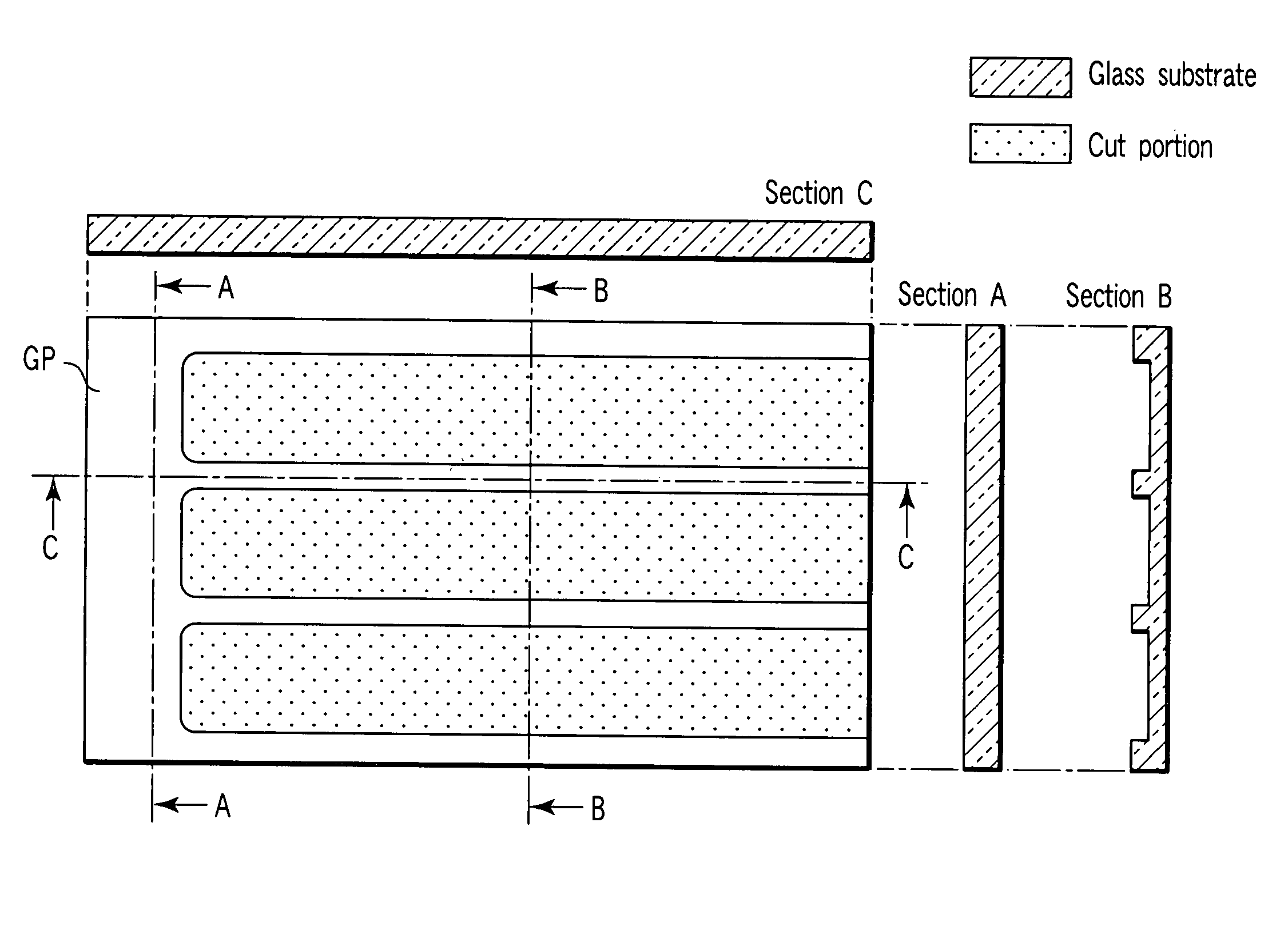
[0024] The first embodiment is directed to a specimen stage array fabricated by machining a glass plate. Machining of the glass plate employs a dicing saw, a diamond cutter, or the like. The specimen stage array according to this embodiment is fabricated in accordance with the following processing procedure.
[0025] First, as shown in FIG. 1, a glass plate GP is cut down in the surface that will be specimen fixing surfaces except for the left end part with a constant width and a constant depth in the direction of a section C and at intervals in the direction of a section B.
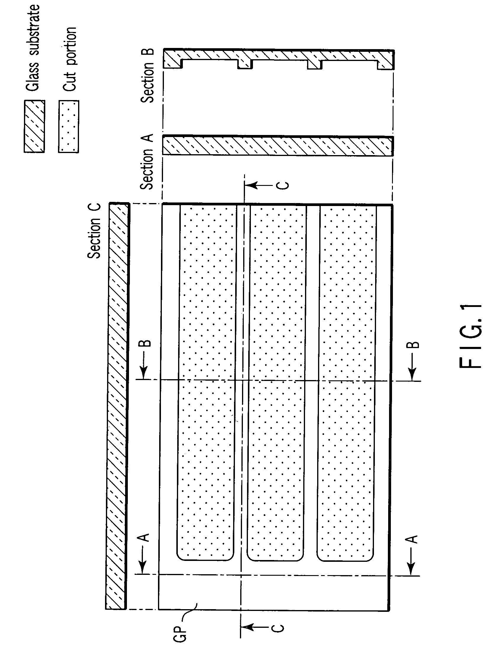
[0026] As shown in FIG. 2, the surface that will be specimen fixing surfaces is cut down with a constant width and a constant depth in the direction of the section B and at intervals in the direction of the section C.
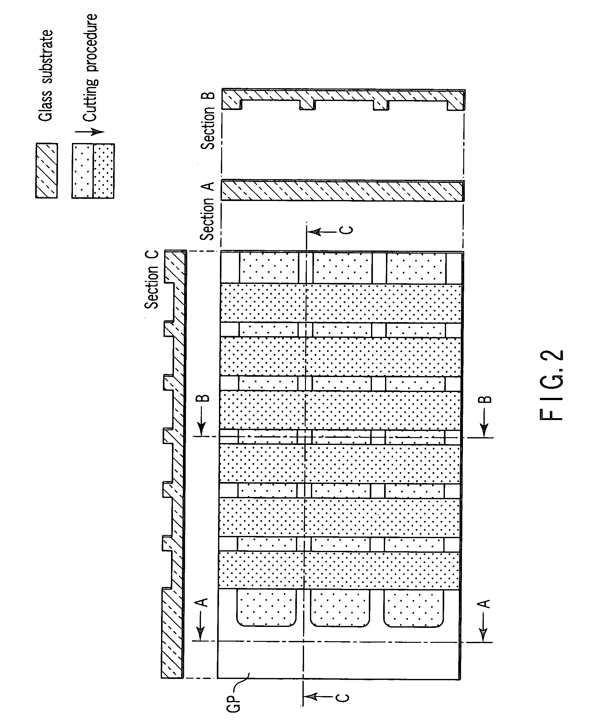
[0027] Subsequently, as shown in FIG. 3, an inner part of each portion that has been cut in the process of FIG. 2 is cut down with a constant width and a constant depth in the direction of the sectio...
second embodiment
[0034] The second embodiment is directed to a specimen stage array that is fabricated using a silicon process. As shown in FIG. 7, a specimen stage array 20 according to this embodiment has specimen stages 22, a frame 24 surrounding the specimen stages 22, and bridge portions 26 connecting the specimen stages 22 and the frame 24. This specimen stage array is fabricated from a semiconductor substrate such as a silicon substrate using the MEMS technique such as a masking process, isotropic and anisotropic etching, and the like. As is apparent from a section A, the specimen stages 22 to the frame 24 are integrally connected by the bridge portions 26.
[0035] Since specimen stage 22 of the second embodiment is thinner than the specimen stage 12 of the first embodiment, when the specimen stage 22 is applied to a high-speed AFM that is installed to match the height of the specimen stages 12 of glass of the first embodiment, the specimen stage 22 is not directly adhered to a Z scanner 18, b...
third embodiment
[0038] The third embodiment is directed to a specimen stage array that is fabricated by arraying specimen stages on a holding member. As shown in FIG. 9, a specimen stage array 30 according to this embodiment comprises specimen stages 32 and a holding member 34 to hold the specimen stages 32. The holding member 34 comprises a film having an adhesive surface. The specimen stages 32 are arranged on the holding member 34 at constant intervals, and their scanner contact surfaces are adhered to the adhesive surface of the holding member 34. All the specimen stages 32 are held on the holding member 34 so that they have the same height. As a result, the specimen fixing surfaces of all the specimen stages 32 are included in a common plane. The holding member 34 may comprise a plate member coated with an adhesive material in place of the film having the adhesive surface.
[0039] In the specimen stage array 30 according to the third embodiment, the holding member 34 holds all the specimen stag...
PUM
| Property | Measurement | Unit |
|---|---|---|
| height | aaaaa | aaaaa |
| atomic force microscope | aaaaa | aaaaa |
| AFM | aaaaa | aaaaa |
Abstract
Description
Claims
Application Information