
Method and apparatus for redundant memory configuration in voltage island

Inactive Publication Date: 2007-05-17
IBM CORP
View PDF5 Cites 13 Cited by
  • Summary
  • Abstract
  • Description
  • Claims
  • Application Information

AI Technical Summary

Benefits of technology

[0018] An object of the present invention is therefore to provide a means for avoiding a condition where memories cannot be accessed in another module upon turning on a predetermined module in a voltage island without providing a fuse cell for each voltage domain (module).

Problems solved by technology

Accordingly, when a failure is found in an installed memory element during manufacturing test of the SoC, the defective memory elements are replaced with redundant memory elements (redundant bits).
However, when memory array redundancy is implemented on a SoC with different voltage islands, the following problems arise.
However, since the configuration information on the memories residing in module 820 is lost, a fuse / decompression module must be initialized again to use the memories.
However, such a configuration leads to an increase in the total area of a chip since a plurality of fuse / decompression modules which occupy an extremely large area on the chip are provided, and also since the effect of compressing data retained by fuse cells weakens due to the scattering of the fuse cells.

Method used


Image

  • Method and apparatus for redundant memory configuration in voltage island
  • Method and apparatus for redundant memory configuration in voltage island
  • Method and apparatus for redundant memory configuration in voltage island

Examples


Embodiment Construction

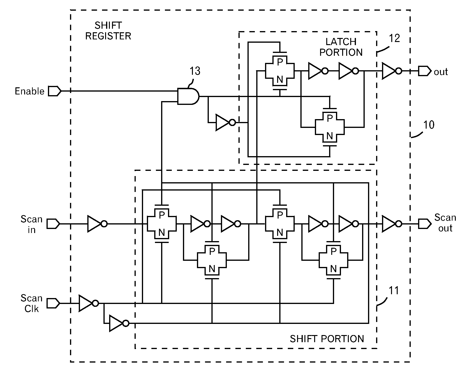
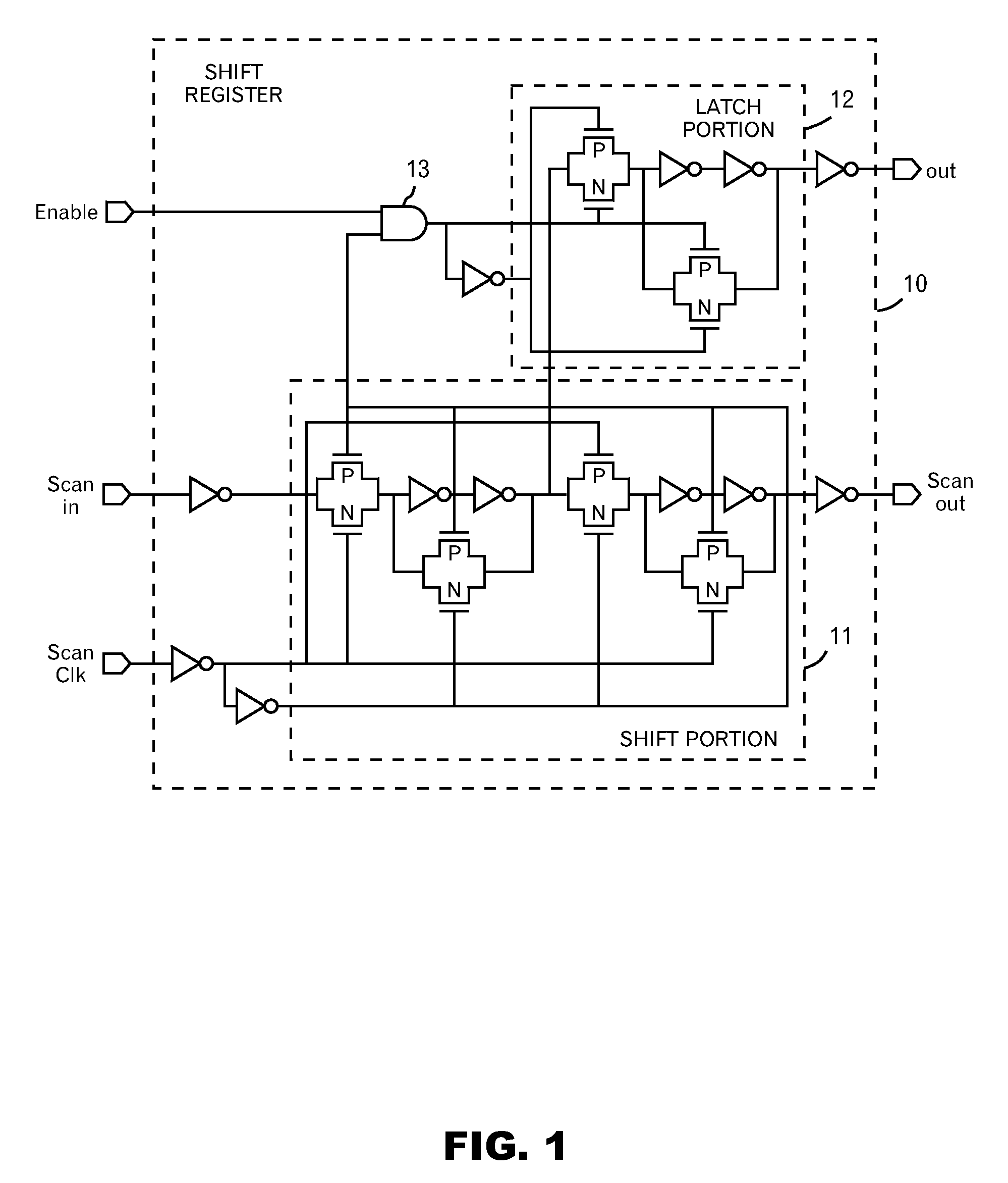
[0034] Hereinafter, with reference to the attached drawings, a detailed description will be given of a best mode for carrying out the present invention (hereinafter, referred to as a first embodiment).

[0035] According to a first embodiment, a scan chain for propagating configuration information to each memory on a SoC is implemented with shift registers (flip-flop circuits) including shift portions and latch portions with new configurations. Moreover, a control circuit for controlling the operations of the shift registers is provided in each domain (module) on the SoC to which voltage islands are applied. A control is achieved in a manner of writing the configuration information on the memories in a predetermined module alone (that is, without influencing another module) with such a configuration, when power is switched on from off in the module.

[0036]FIG. 1 is a view showing a circuit configuration of the shift register according to a first embodiment.

[0037] Shift register 10 sh...


PUM


Abstract

A method and apparatus to configure redundant memory elements in a system on a chip (SoC) having discrete voltage domains (islands). A plurality of memories are provided for each voltage island, each containing redundancy elements or having the capability to access redundant memory elements in a neighboring voltage domain; a fuse cell stores configuration information for controlling the switching of memory elements of the plurality of memories; a shift register receives and retains configuration information on a memory array from the fuse cell corresponding to each memory; and a control circuit directs operation of the shift register. The shift register includes a shift portion for receiving the data of the configuration information and transferring the data to another shift register, and a latch portion for retaining the data inputted to the shift portion. The control circuit controls whether or not the data of the shift register, which is inputted to the shift portion, is to be retained in the latch portion.

Description

BACKGROUND OF THE INVENTION [0001] The present invention relates to a microcomputer configured in a single chip, which is provided with a plurality of modules activated by causing power to be supplied from an independent power source, and particularly relates to the control over its memories. [0002] As the integration of an LSI device progresses, a chip configuring a system on silicon that is, a LSI called a System on Chip (SoC) has been realized. [0003] The SoC often includes a memory inside the chip. With increasing storage capacity of the SoC memory, redundancy schemes implemented in the memory are instrumental in improving chip manufacturing yields (for example, refer to Japanese Patent Application Laid-open No. Hei 7-320495 and incorporated herein by reference). Accordingly, when a failure is found in an installed memory element during manufacturing test of the SoC, the defective memory elements are replaced with redundant memory elements (redundant bits). The replacement of me...

Claims


Application Information

Patent Timeline
IPC IPC(8): G11C29/00
CPCG11C29/789
Inventor TANIGUCHI, MASAYOSHIMASHIMA, ISAMUUSAMI, JUN
Owner IBM CORP
Learn More