

Design method for semiconductor integrated circuit
a technology of integrated circuits and design methods, applied in the direction of semiconductor devices, electrical equipment, basic electric elements, etc., can solve the problem of insufficient level of accuracy, and achieve the effect of improving simulation accuracy, high accuracy, and reducing the stress of adjacent cells
- Summary
- Abstract
- Description
- Claims
- Application Information
AI Technical Summary
Benefits of technology
Problems solved by technology
Method used
Image

Examples
first embodiment
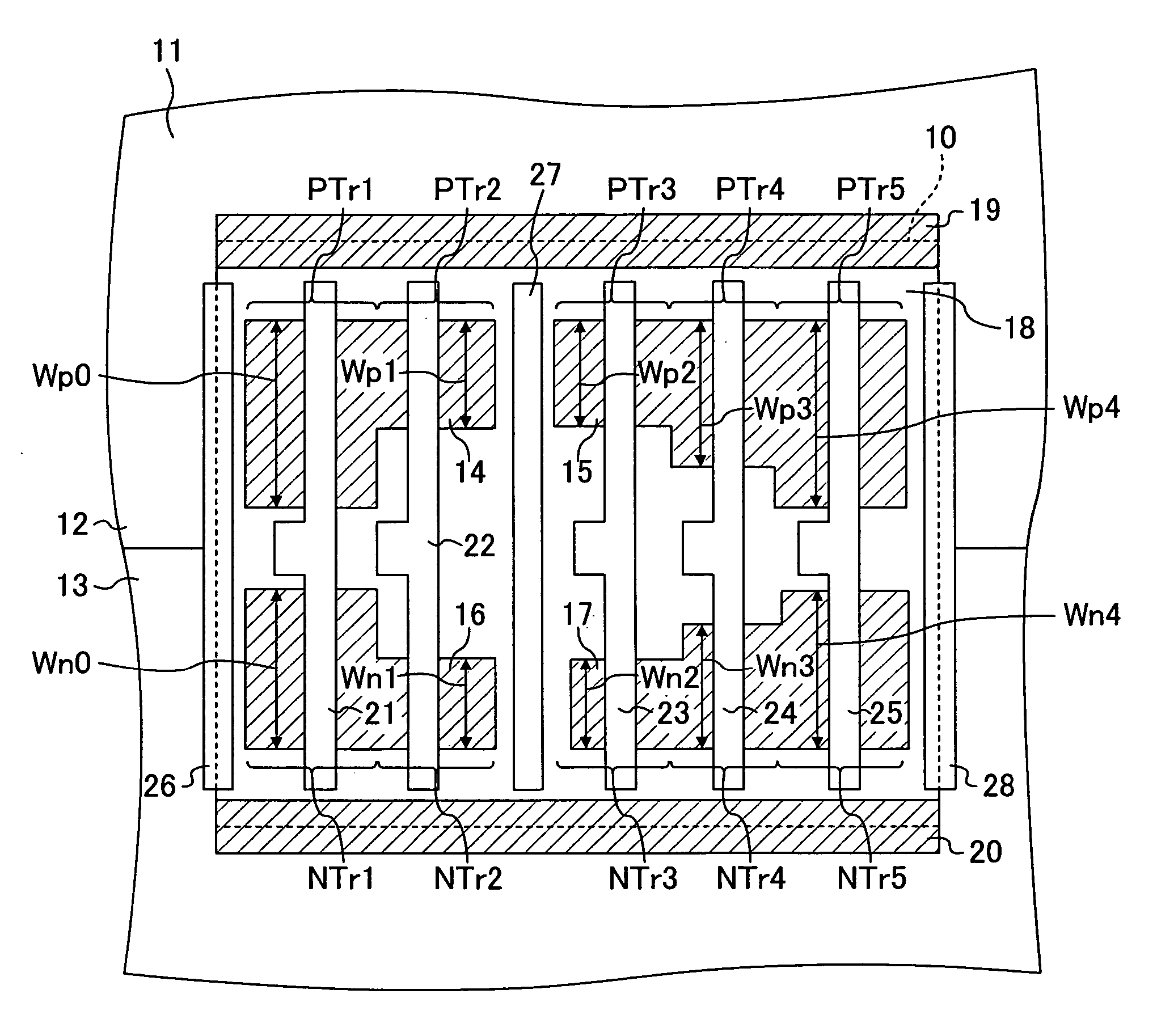
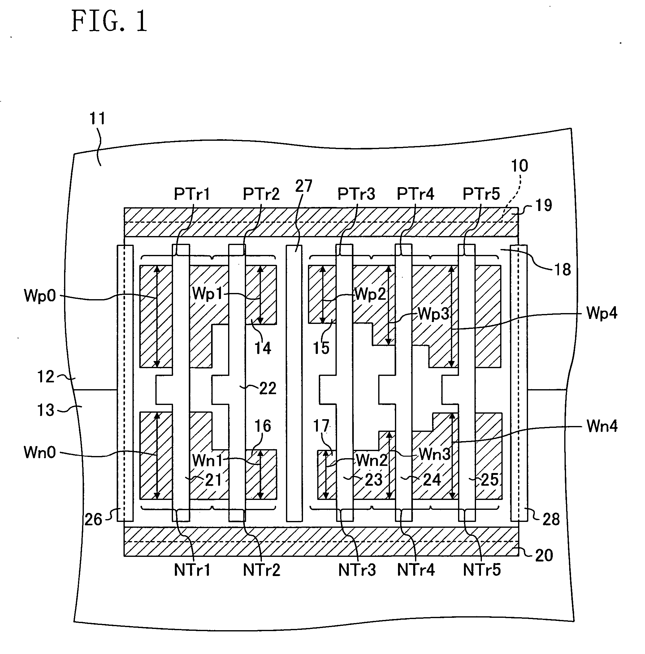
[0045] Hereinafter, a semiconductor circuit device designing method according to a first embodiment of the present invention will be described with reference to the accompanying drawings. FIG. 1 is a plan view illustrating a structure of a standard cell according to the first embodiment of the present invention. Note that the standard cell (or cell) as used herein refers to a range within which CMIS transistors are arranged and connected so as to achieve one or more functions (e.g., logical inversion, logical AND, etc.). A system LSI is designed by providing several hundreds of kinds of standard cells and performing wiring between the standard cells. In general, simulation is performed with respect to a system LSI using a hierarchy. For each of the several hundreds of kinds of standard cells, simulation is performed to create a table of delay information, and the delay information is used to perform simulation at the block level and the chip level.
[0046] In FIG. 1, a boundary betwe...
second embodiment
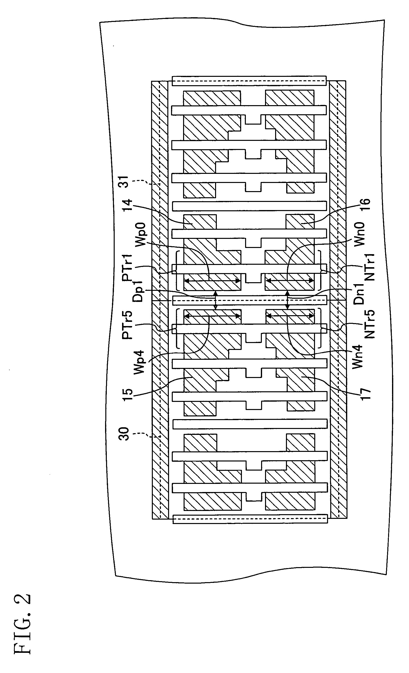
[0063] Hereinafter, a semiconductor circuit device designing method according to a second embodiment of the present invention will be described with reference to the drawings. FIG. 4 is a plan view illustrating a structure of a standard cell according to a second embodiment of the present invention. In the structure of FIG. 4, a plurality of the standard cells 10 of FIG. 1 are arranged in an array.
[0064] In FIG. 4, a boundary between each standard cell 10 is indicated by a dashed line. Note that an arrangement of gate conductors and active areas in the standard cell 10 is similar to that of FIG. 1, and will not be described in detail.
[0065] At the present time, LSIs are generally designed using a cell-based technique. In this method, cells are provided at lattice points, and input and output terminals (not shown) in the standard cell 10 are connected using conductors (not shown). This design is automatically performed using an EDA tool (tool for arranging cells and connecting the ...
PUM
 Abstract
Description
Claims
Application Information