Compound-Eye Imaging Device

a compound eye and imaging technology, applied in the field of compound eye imaging devices, can solve the problems of increasing power consumption, difficult to obtain a sufficiently high frame rate, increasing clock frequency, etc., and achieves the effect of easy enabling a high frame rate, high resolution, and increasing clock frequency

Inactive Publication Date: 2007-05-24
FUNAI ELECTRIC CO LTD
View PDF5 Cites 32 Cited by
  • Summary
  • Abstract
  • Description
  • Claims
  • Application Information

AI Technical Summary

Benefits of technology

[0009] An object of the present invention is to provide a compound-eye imaging device that easily enables a high frame rate and imaging at a high resolu...

Problems solved by technology

Thus, if an attempt is made to display a reconstructed image on a display screen such as an LCD (Liquid Crystal Display) monitor at a relatively high frame rate (number of images renewed per unit time), it is required to increase the reading speed to read the single-eye images from the photodetector array This makes it necessary to increase the clock frequency of the microprocessor, which caus...

Method used


Image

  • Compound-Eye Imaging Device
  • Compound-Eye Imaging Device
  • Compound-Eye Imaging Device

Examples


Embodiment Construction

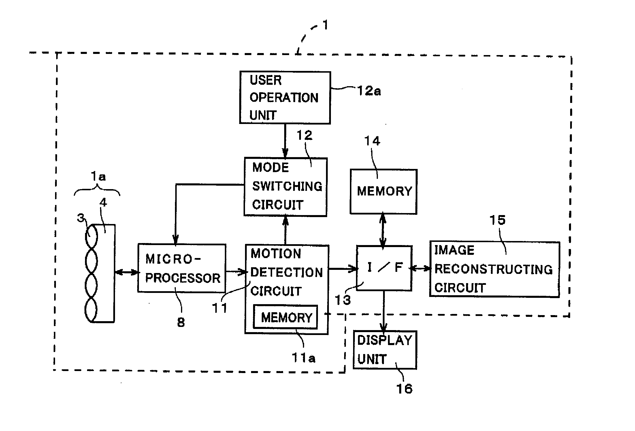
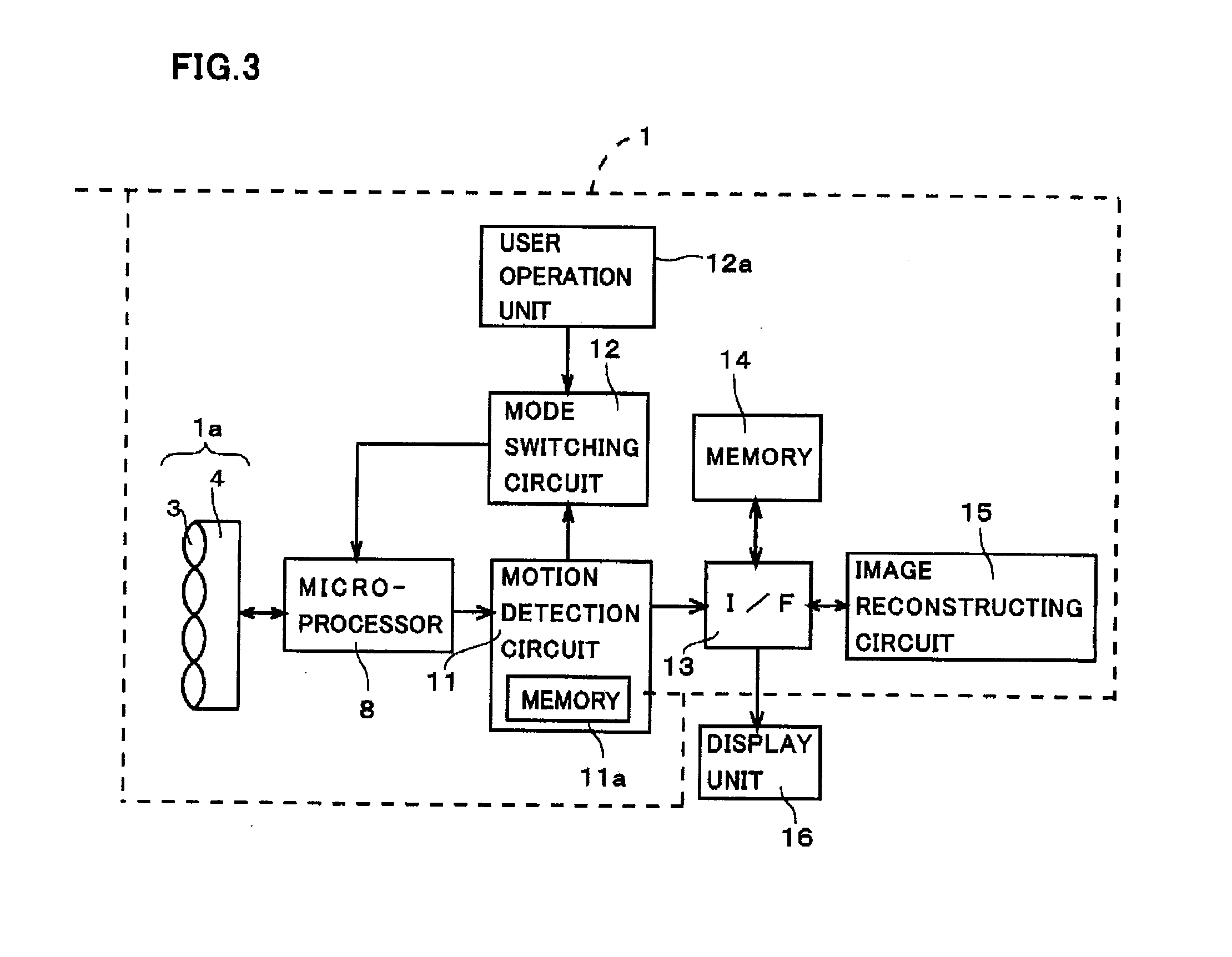
[0024] Embodiments of the present invention, as best mode for carrying out the invention, will be described hereinafter with reference to the drawings. The present invention relates to a compound-eye imaging device. The following embodiments describe examples in which the compound-eye imaging device of the present invention is used as an imaging device for a monitoring camera system, first of all, as well as a cellular phone and a face authentication system. It is to be understood that the embodiments described herein are not intended as limiting, or encompassing the entire scope of, the invention. Note that like parts are designated by like reference numerals or characters throughout the drawings.

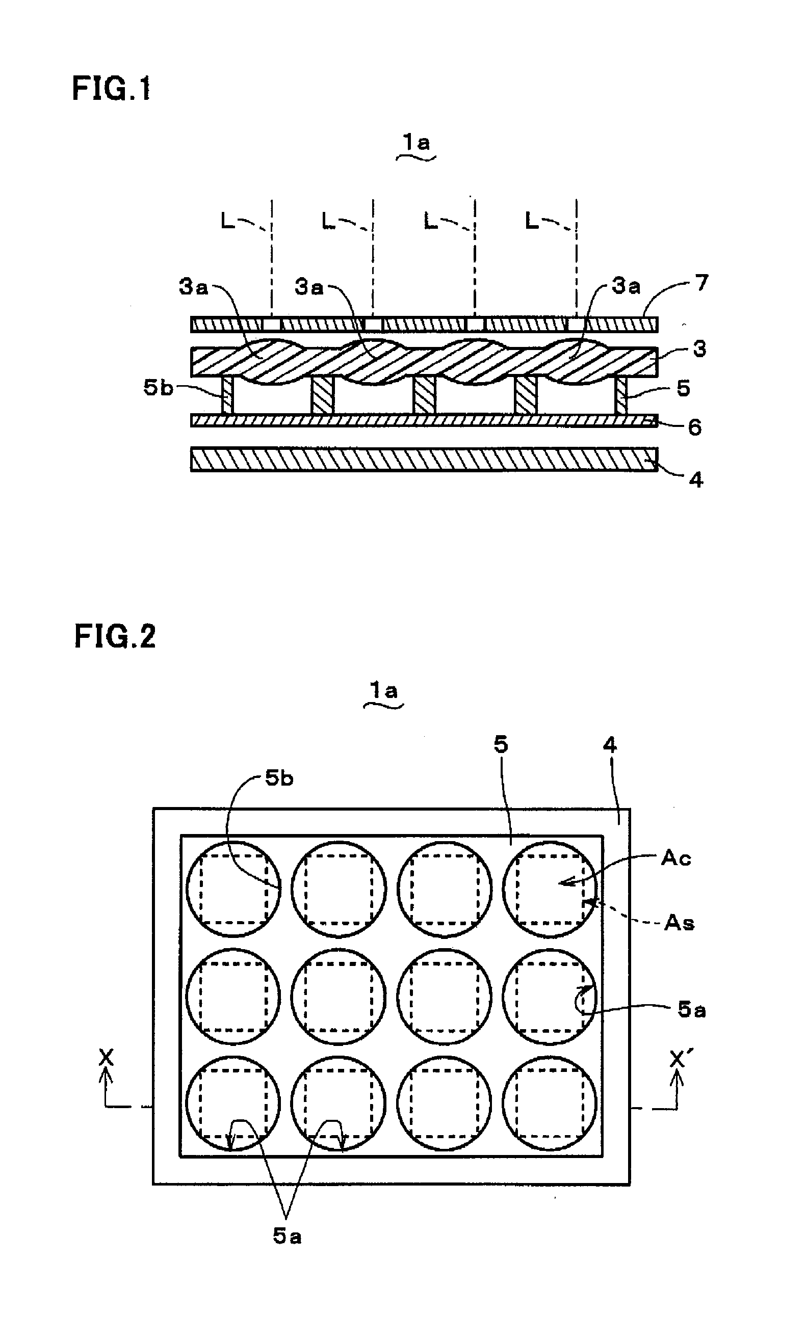
[0025]FIG. 1 is a schematic side cross-sectional view of an optical imaging unit la along line X-X′ of FIG. 2 to be used for a compound-eye imaging device 1 (refer to FIG. 3) according to an embodiment of the present invention, while FIG. 2 is a schematic plan view of the optical imaging ...


PUM


Abstract

A compound-eye imaging device comprising: an optical lens array with multiple integrated optical lenses having mutually parallel optical axes; a photodetector array placed at a predetermined distance from the optical lens array for imaging multiple images (referred to as single-eye images) formed by the optical lenses; and a microprocessor for reading the single-eye images imaged by the photodetector array. The image reading mode of the microprocessor is switchable between an all-read mode in which all the single-eye images on the photodetector array are sequentially read, and a partial-read mode in which a part of the single-eye images thereon are selectively read. The image reading speed of the microprocessor is changeable. The compound-eye imaging device enables a high frame rate and a high resolution imaging while reducing an increase in a clock frequency for the frame rate and thus reducing an increase in power consumption.

Description

BACKGROUND OF THE INVENTION [0001] 1. Field of the Invention [0002] The present invention relates to a compound-eye imaging device having an optical imaging system formed of multiple micro optical systems, in which multiple images imaged by the micro optical systems are reconstructed into one image. [0003] 2. Description of the Related Art [0004] There has been developed a compound-eye imaging device as a thin camera module to be installed in a cellular phone, a personal computer, or the like. The compound-eye imaging device is mainly composed of: an optical lens array with multiple integrated optical lenses having mutually parallel optical axes; a photodetector array for imaging multiple images (single-eye images) formed by the respective optical lenses of the optical lens army; and an image reconstructing circuit for reconstructing one image from the multiple single-eye images imaged by the photodetector array by using parallax information between the multiple single-eye images. [...

Claims


Application Information

Patent Timeline
IPC IPC(8): G01J1/00H04M1/00H04N5/225H04N5/232H04N5/335
CPCG02B3/0006G02B3/0068G02B3/0075H04N5/2254H04N5/2257H04N5/232H04N5/23245H04N5/772H04N23/57H04N23/667
Inventor NAKAO, YOSHIZUMITOYODA, TAKASHIMASAKI, YASUO
Owner FUNAI ELECTRIC CO LTD
Why Eureka
Try Eureka