Optical logic device

Inactive Publication Date: 2007-05-24
JOSHI ADITYA NARENDRA
View PDF60 Cites 8 Cited by
  • Summary
  • Abstract
  • Description
  • Claims
  • Application Information

AI Technical Summary

Problems solved by technology

However, there are a myriad of challenges before technologists to accomplish such advanced goals.
In particular the creation of suitable optical logic circuits has challenged computer technologists giving rise to a need for improved optical switches that can operate individually or be made into logic gates or other information processing constructions.

Method used


Image

  • Optical logic device
  • Optical logic device
  • Optical logic device

Examples


Embodiment Construction

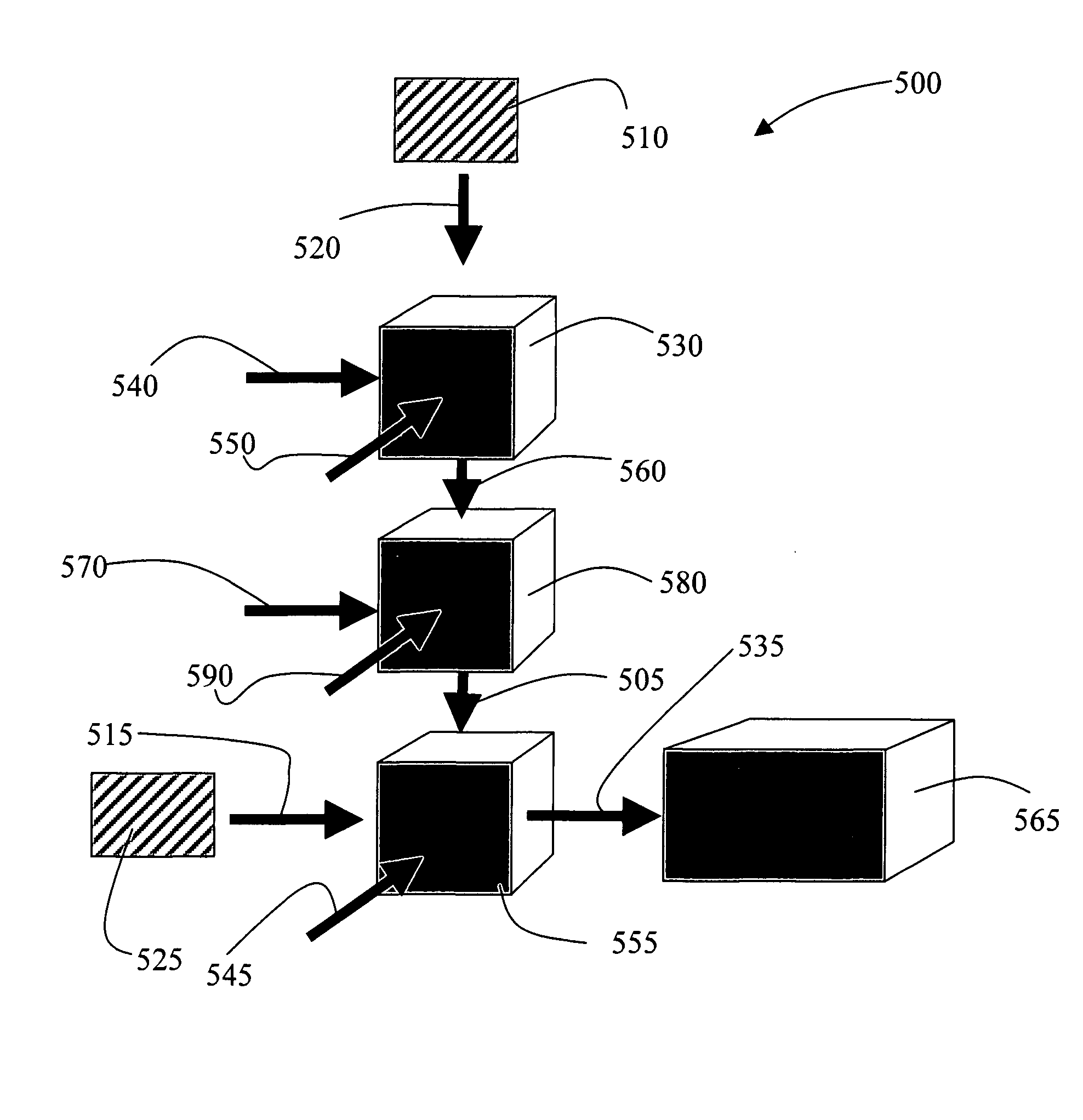
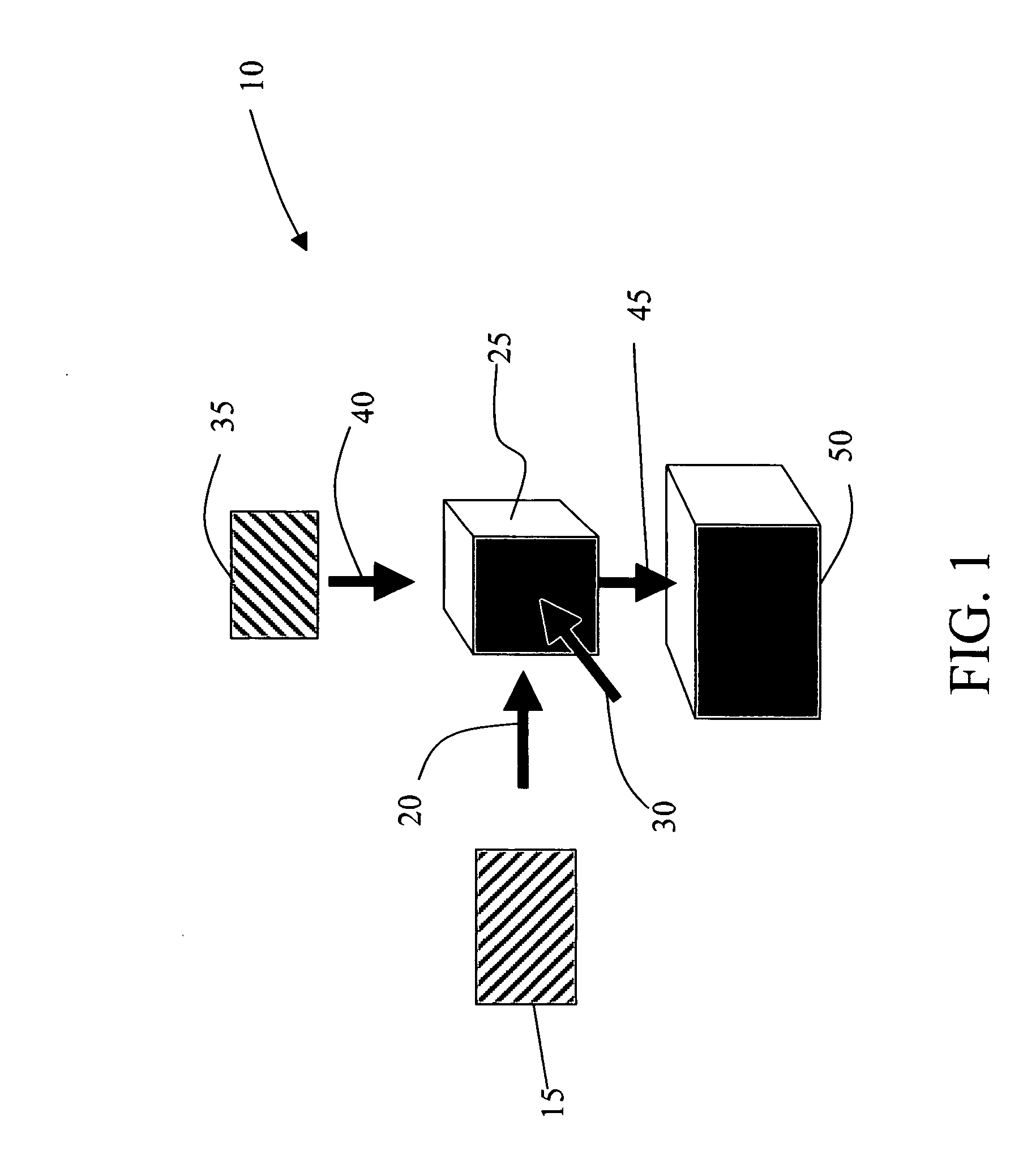
[0018] The invention pertains to the use of optically active dyes such as rhodamine, coumarin or other optically active materials to perform processing functions on optical data. The data is carried in pulses of photons of wavelengths appropriate to interact with and excite or de-excite the optically active materials.

[0019] The invention utilizes dye cells such as those made using commercially available rhodamine 6G, coumarin, other fluorescent dyes, or other optically active material. A dye cell is pumped using a laser or other suitable pump to raise the dye atoms and or molecules from a low energy state, also called a de-excited state or a ground state, to an excited state. The data pulse, also called data signal, which has a wavelength in the active region of the laser dye, then enters the dye cell. If the data pulse is high in energy, designated as 1 or High, the signal stimulates the excited optical material in the cell and depletes the number of excited species in the cell ve...


PUM


Abstract

The invention uses optically active dyes or other optically active materials to perform digital data processing and logic functions on optical data. The data is carried in pulses of photons of wavelengths appropriate to interact with the optically active materials to excite or de-excite them. The use of the invention in performing various optical processing functions is described.

Description

CROSS REFERENCE TO RELATED APPLICATION [0001] This application claims the benefit of co-pending U.S. Provisional Patent Application No. 60 / 738,467 filed Nov. 21, 2005.BACKGROUND OF THE INVENTION [0002] The invention relates to the use of active optical materials to perform logic operations using optical signals. [0003] In the field of digital electronics, specific logic functions are performed by electronic circuits. These logic functions are commonly known by those skilled in the art of digital electronics. Examples of the logic functions and their electronic analogs are known as the AND gate, the NAND gate, the OR gate, the NOR gate and various other logic based circuits that can be designed to perform particular electronic functions. These functions are based on a truth table or logic table that defines the output when a set of selected input conditions are present. It is possible to design electronic circuits so that they replicate the results of these truth tables. In these des...

Claims


Application Information

Patent Timeline
IPC IPC(8): G06E3/00G02F3/00
CPCG02F3/00G06E1/00
Inventor JOSHI, ADITYA
Owner JOSHI ADITYA NARENDRA
Why Eureka
Try Eureka