Strained silicon on insulator (SSOI) with layer transfer from oxidized donor

a technology of oxidized donor and strained silicon, which is applied in the direction of basic electric elements, electrical apparatus, semiconductor devices, etc., can solve the problems of inconvenient production of inconvenient to achieve the thickness requirements for fully depleted strained semiconductors on insulators, and inconvenient structur

Inactive Publication Date: 2007-05-24
MEMC ELECTONIC MATERIALS INC
View PDF16 Cites 32 Cited by
  • Summary
  • Abstract
  • Description
  • Claims
  • Application Information

AI Technical Summary

Problems solved by technology

Such a structure has limitations, however.
For example, it is not conducive to the production of fully-depleted strained semiconductor on insulator devices in which the layer over the insulating material must be thin enough (e.g., less than 300 angstroms) to allow for full depletion of the layer during device operation.
Additionally, the relaxed SiGe layer adds to the total thickness of the layer over

Method used


Image

  • Strained silicon on insulator (SSOI) with layer transfer from oxidized donor
  • Strained silicon on insulator (SSOI) with layer transfer from oxidized donor
  • Strained silicon on insulator (SSOI) with layer transfer from oxidized donor

Examples


example

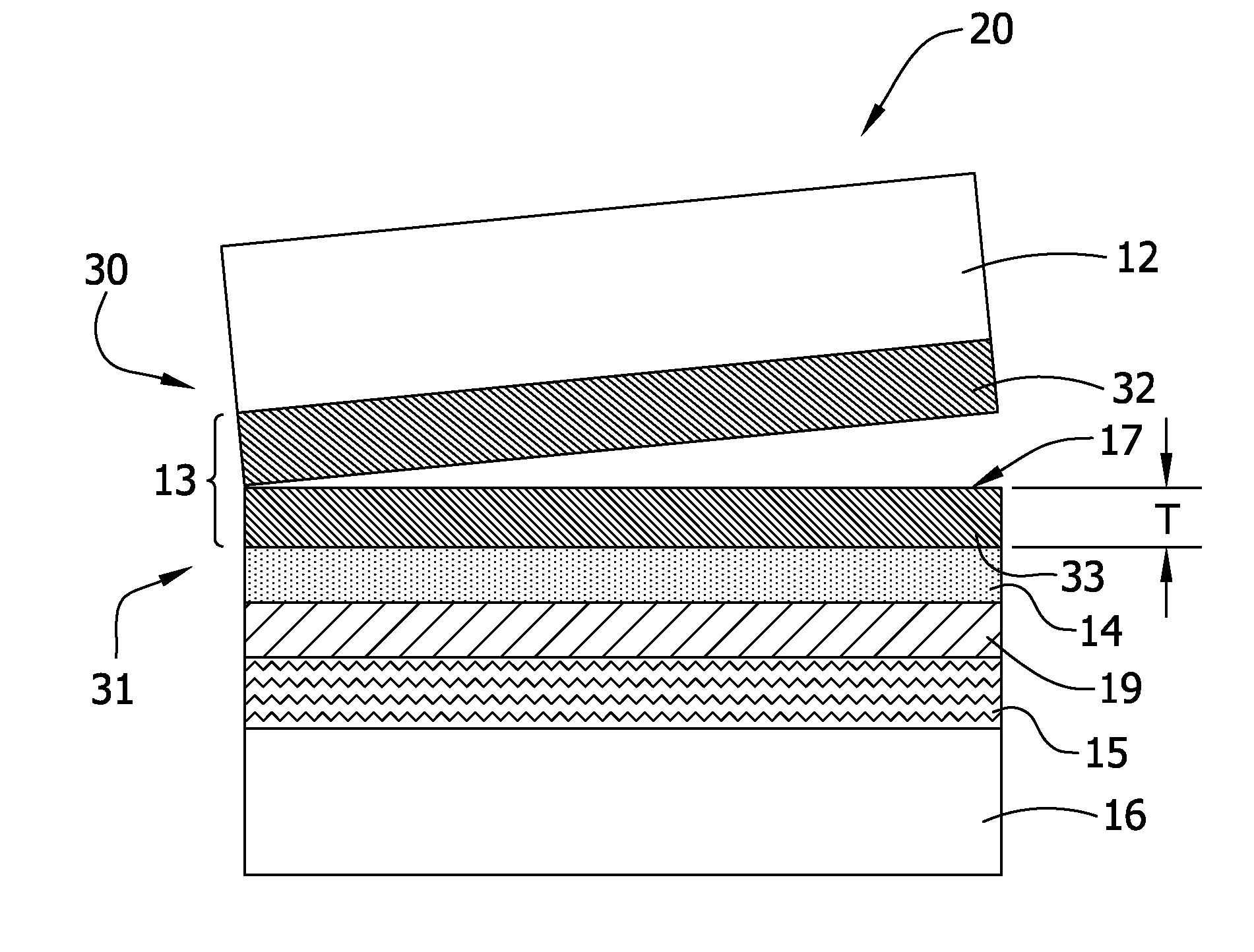
[0063] A silicon donor wafer structure was prepared according to the invention by depositing a relaxed SiGe layer having an average thickness of about 0.2 μm via a commercial epitaxial deposition process utilizing a Ge-source gas and a Si-source gas. This was followed by applying a layer of silicon having an average thickness of about 80 nm thereon by means of epitaxial growth in an ASM Epislon 1 single wafer reactor. The silicon donor wafer was then subjected to an oxidation process, wherein the donor wafer was exposed to an atmosphere comprising steam at a temperature of about 800° C. for 360 seconds. This anneal produced a thin layer of SiO2 that had an average thickness of about 50 Å on the surface of the strained silicon layer. A combination of hydrogen and helium ions were then implanted into the SiGe layer, through the strained silicon layer and the SiO2 layer, to a depth of approximately 120 nm by an external implant service (Innovion Corporation), to create a separation pla...


PUM


Abstract

This invention generally relates to a strained silicon on insulator (SSOI) structure, and to a process for making the same. The process includes forming a thin SiO2 layer on a strained silicon layer after it is formed on the donor wafer and before bonding to the handle wafer.

Description

REFERENCE TO RELATED APPLICATIONS [0001] This application is a continuation-in-part of pending U.S. patent application Ser. No. 11 / 461,653, filed Aug. 1, 2006, which claims priority from U.S. Provisional Application Ser. No. 60 / 705,039 filed on Aug. 3, 2005, the entire disclosures of which are incorporated herein by reference.FIELD OF THE INVENTION [0002] The present invention relates generally to a strained silicon on insulator (SSOI) structure. More particularly, the present invention is directed to a SSOI structure with an improved bond interface between the strained silicon layer and the handle wafer. The present invention is further directed to a process for making such a structure. BACKGROUND OF THE INVENTION [0003] Silicon on insulator (SOI) structures generally comprise a handle wafer, a semiconductor device layer, and a dielectric insulating layer between the handle wafer and the device layer. By insulating the device layer from the handle wafer of the SOI structure, the de...

Claims


Application Information

Patent Timeline
IPC IPC(8): H01L27/12H01L21/30
CPCH01L21/30604H01L21/76254
Inventor SEACRIST, MICHAEL R.FEI, LU
Owner MEMC ELECTONIC MATERIALS INC
Why Eureka
Try Eureka