Method of forming contact

Active Publication Date: 2007-05-24
UNITED MICROELECTRONICS CORP
View PDF1 Cites 4 Cited by
  • Summary
  • Abstract
  • Description
  • Claims
  • Application Information

AI Technical Summary

Benefits of technology

[0012] Accordingly, at least one objective of the present invention is to provide a method of forming a contact that can prevent the degradation of device performance resulting from the formation of residue at the bottom of a contact opening due to the presence of defects in the film layers.
[0013] At least another objective of the present invention is to provide a method of forming a contact that can prevent the degradation of device performance due to the formation of defects in the stress layer.
[0022] In the present invention, the width of the seam in the first dielectric layer (or the stress layer) is expanded. Thus, residue is prevented from forming at the bottom of the contact opening. Therefore, the resistance of the contact will not increase. Moreover, the drop in the reliability and performance of the device due to short circuit is substantially minimized as well.

Problems solved by technology

However, the miniaturization of devices has encountered a barrier due to a bottleneck in the fabrication technique and an increase in production cost.
Nevertheless, the aforesaid method has some problems that are difficult to remove.
Thus, the overall performance of the device is still substantially limited.
Sometimes, a short circuit between the contact 116 and the MOS transistor 102 may form resulting in a significant drop in the reliability and performance of the device.

Method used


Image

  • Method of forming contact
  • Method of forming contact
  • Method of forming contact

Examples


Embodiment Construction

[0031] Reference will now be made in detail to the present preferred embodiments of the invention, examples of which are illustrated in the accompanying drawings. Wherever possible, the same reference numbers are used in the drawings and the description to refer to the same or like parts.

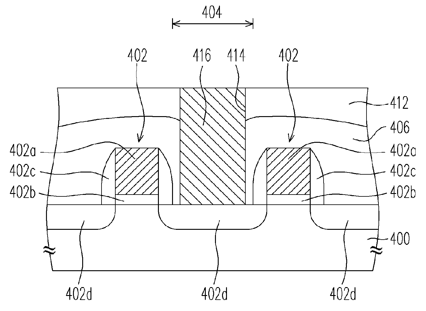
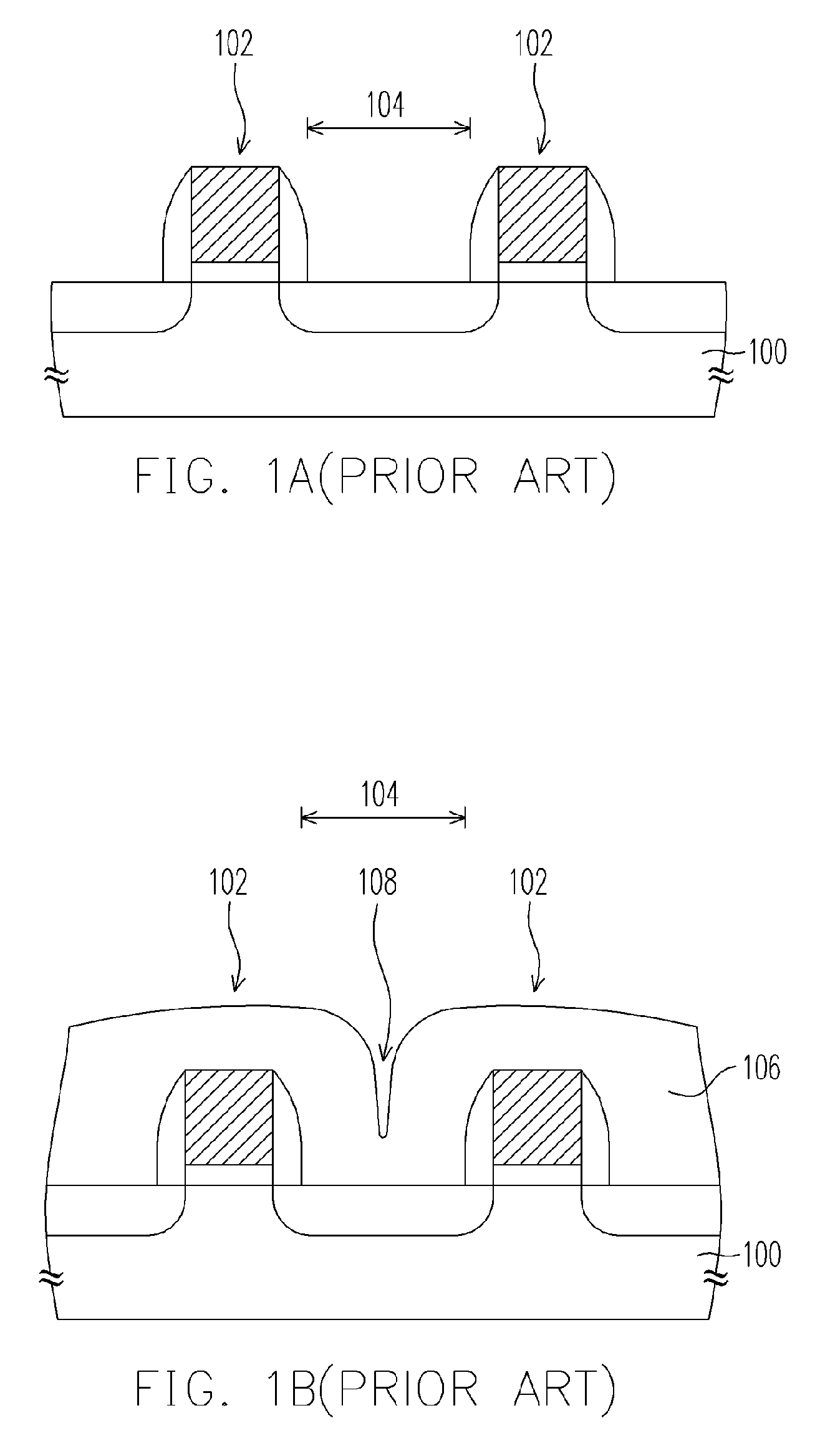
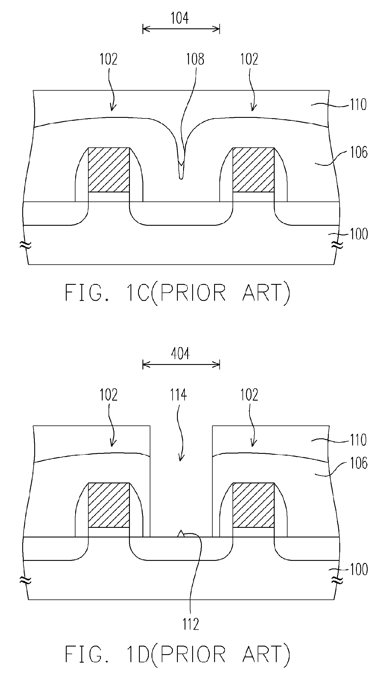
[0032]FIGS. 4A through 4F are schematic cross-sectional views showing the method of forming a contact according to one embodiment of the present invention. First, as shown in FIG. 4A, a substrate 400 having at least two conductive devices 402 is provided. Furthermore, there is a spacing 404 between two adjacent conductive devices 402. The conductive device 402 can be a metal-oxide-semiconductor (MOS) transistor, for example. Each MOS transistor comprises a gate 402a, a gate dielectric layer 402b, a pair of spacers 402c and a pair of source / drain regions 402d, for example.

[0033] As shown in FIG. 4B, a dielectric layer 406 is formed over the substrate 400. The dielectric layer 406 covers the entire ...


PUM


Abstract

A method of forming a contact is provided. A substrate having at least two conductive devices is provided. A spacing is located between the two conductive devices. A first dielectric layer is formed over the substrate to cover the two conductive devices and the spacing. A seam is formed in the first dielectric layer within the spacing. Then, a portion of the first dielectric layer is removed to form an opening so that the width of the seam is expanded. A second dielectric layer is formed over the first dielectric layer to fill the opening. A portion of the second dielectric layer and a portion of the first dielectric layer within the spacing are removed until a portion of the surface of the substrate is exposed and a contact opening is formed in the location for forming the contact. Finally, conductive material is deposited to fill the contact opening.

Description

BACKGROUND OF THE INVENTION [0001] 1. Field of the Invention [0002] The present invention relates to a method of forming a semiconductor device. More particularly, the present invention relates to a method of forming a contact. [0003] 2. Description of the Related Art [0004] In the development of integrated circuits, a device can operate faster at a lower power rating through a reduction in the size of the device. However, the miniaturization of devices has encountered a barrier due to a bottleneck in the fabrication technique and an increase in production cost. As a result, other types of miniaturization techniques have been developed to improve the driving current of devices. One proposed solution to relieve the limit of device miniaturization includes controlling the stress at the channel region of a transistor. Through the application of some stress, the distance between silicon atoms in the silicon crystal is reduced so that the mobility of electrons and holes are increased. Ul...

Claims


Application Information

Patent Timeline
IPC IPC(8): H01L21/4763
CPCH01L21/76802H01L21/76829H01L21/76837
Inventor YANG, CHAO-LONCHEN, NENG-KUOTSAI, TENG-CHUNHUANG, CHIEN-CHUNGHSU, SHAO-TA
Owner UNITED MICROELECTRONICS CORP
Why Eureka
Try Eureka