

Organic photoelectric conversion device and stack type photoelectric conversion device
a photoelectric conversion device and organic technology, applied in the direction of organic semiconductor devices, photoelectric discharge tubes, instruments, etc., can solve the problems of large dark current and other problems, and achieve the effects of reducing dark current, low noise, and high light transmittan
- Summary
- Abstract
- Description
- Claims
- Application Information
AI Technical Summary
Benefits of technology
Problems solved by technology
Method used
Image

Examples
example 1
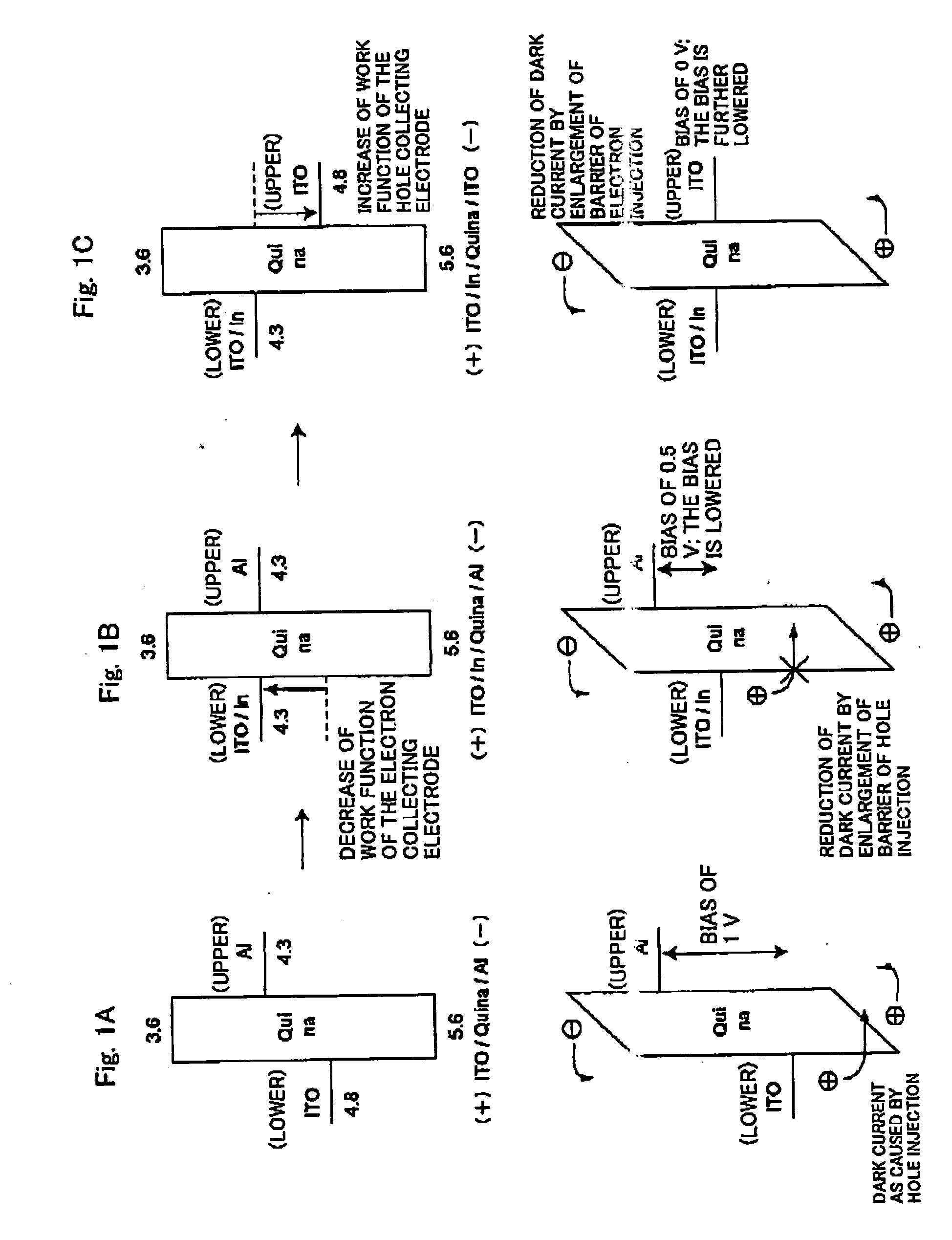
FIG. 1B
[0125] On the other hand, a device was prepared in the same manner as in Comparative Example 1, except for using, as the lower electrode, an electrode as prepared by stacking In having a small work function as 4.3 eV in a thickness of 2 nm on in ITO electrode by vacuum vapor deposition (visible light transmittance of 2 nm-thick In: about 98%). As a result, the dark current at the applied voltage of 1 V is largely reduced to 1.8 nA / cm2 a value of which is lowered by approximately four digits.
[0126] As illustrated in FIG. 1B, this means that the hole injection from the electron collecting electrode is largely reduced by making the work function of the lower electrode which is the electron collecting electrode small.
[0127] Similarly, light of 550 nm was made incident from the lower ITO side in an irradiation intensity of 50 μW / cm2 under a condition of applying bias of 1 V. As a result, the external quantum efficiency (measured charge number against the incident photo number) ...
example 2
FIG. 1C
[0128] In addition, a device was prepared in the same manner as in Example 1, except for replacing the upper electrode from the Al electrode to an ITO electrode (work function: 4.8 eV; visible region light transmittance: 98%) to adjust the work function, thereby devising to reduce the dark current and realize a low bias. Here, the ITO transparent electrode as the upper electrode was deposited in thickness of 10 nm on an organic layer at 40 W by means of RF magnetron sputtering. At the time of sputtering film formation of ITO, although some devices caused a short circuit due to damage onto the organic layer, some devices which had been able to be successfully fabricated without causing a short circuit were provided for the measurement. Light of 550 nm was made incident from the lower ITO side in an irradiation intensity of 50 μW / cm2. As a result at the applied bias of 2 V, the dark current was 40 nA / cm2, and the external quantum efficiency was 42.
[0129] In comparison with Ex...
example 3
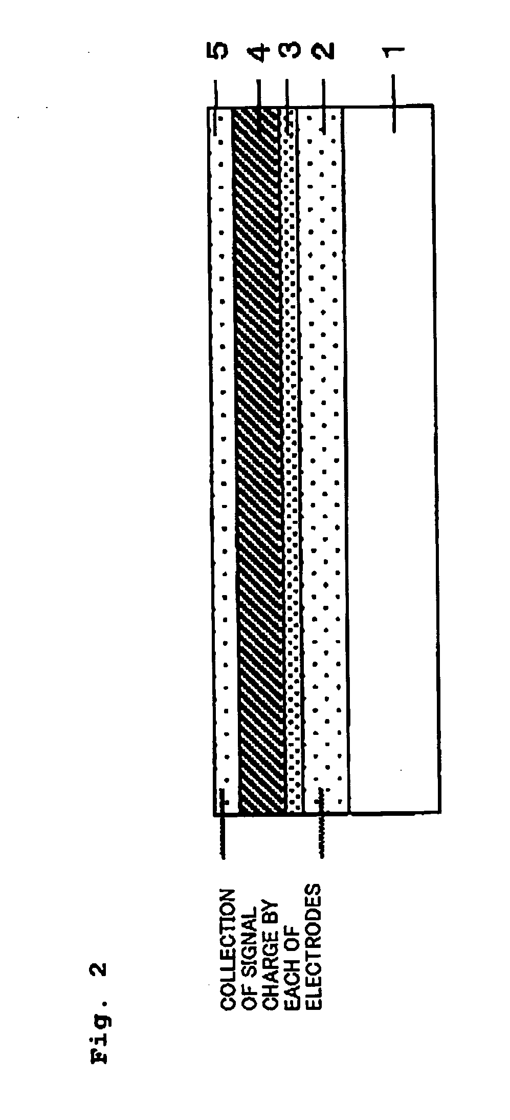
[0130] So far, the results obtained in stacking an In thin layer on an ITO electrode with respect to a device resulting from interposing a quinacridone single layer originally having a large dark current between electrodes have been described. Now, in order to confirm generality, in stacking an In thin layer, too with respect to a device with reduce dark current by a multilayered configuration of an organic material, whether or not the effects are revealed was examined. The configuration of the photoelectric conversion device as examined herein is ITO / BCR (the following Compound 2: 2,9-dimethyl-4,7-diphenyl-1,10-phenathroline) (20 nm) / Alq3 (the following Compound 3: tris(8-hydroxyquinolinato)aluminum(III) complex) (50 nm) / quinacridone (100 nm) / m-MTDATA (the following Compound 4: 4,4′,4″-tris(N-(3-methylphenyl)N-phenylamino)triphenylamine) (5 μnm) / Al (100 nm). When the bias of 10 V was applied to this device, the dark current was 5.6 nA / cm2, and the external quantum efficiency in an...
PUM
 Abstract
Description
Claims
Application Information