Communication semiconductor chip, calibration method, and program

a technology of communication semiconductor and calibration method, which is applied in the direction of semiconductor/solid-state device details, instruments, printed circuit aspects, etc., can solve the problems of increasing the size of the entire semiconductor device, unable to gain an area for the terminals, and the number of terminals of layered boards is limited, so as to achieve a broader communication range and facilitate communication , the effect of stable communication

Inactive Publication Date: 2007-05-31
SONY CORP
View PDF12 Cites 13 Cited by
  • Summary
  • Abstract
  • Description
  • Claims
  • Application Information

AI Technical Summary

Benefits of technology

[0022] Another aspect of the present invention can implement a communication semiconductor chip allowing communication to be performed more easily and more stably.
[0023] Still another aspect of the present invention can implement a communication semiconductor chip allowing communication to be performed in a broader communication range more easily.
[0024] A further aspect of the present invention can provide a calibration method performed on parameters used in a communication semiconductor chip. More specificall...

Problems solved by technology

However, in a method described in the above-cited patent document, the number of terminals of layered boards is limited by the width of a board coupled to a side face of the layered boards (hereinafter, referred to as a “side board”).
However, since...

Method used


Image

  • Communication semiconductor chip, calibration method, and program
  • Communication semiconductor chip, calibration method, and program
  • Communication semiconductor chip, calibration method, and program

Examples


Embodiment Construction

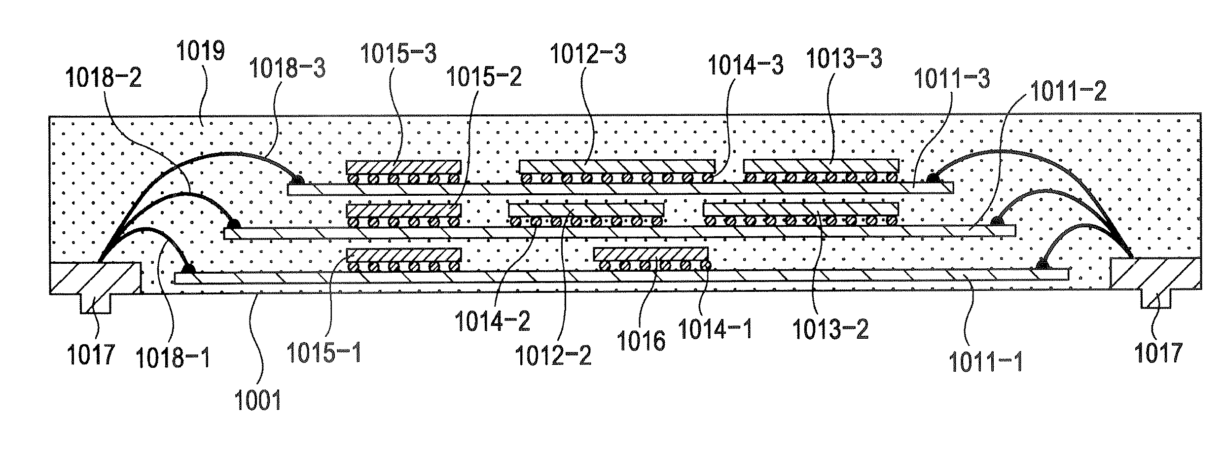
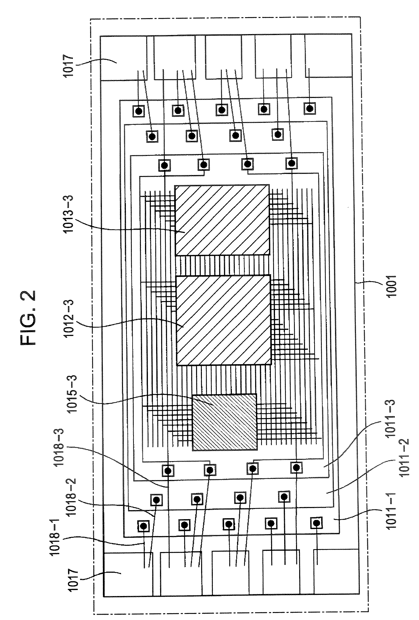
[0062] Before describing an embodiment of the present invention, the correspondence between the features of the present invention and the specific elements disclosed in embodiments described in detailed description of the present invention is discussed below. This description is intended to assure that embodiments supporting the claimed invention are described in the detailed description in this specification. Thus, even if an element in the following embodiments is not described as relating to a certain feature of the present invention, that does not necessarily mean that the element does not relate to that feature of the claims. Conversely, even if an element is described herein as relating to a certain feature of the claims, that does not necessarily mean that the element does not relate to other features of the claims.

[0063] Furthermore, this description should not be construed as restricting that all the aspects of the invention disclosed in the embodiments are described in th...


PUM


Abstract

A communication semiconductor chip performs wireless communication with another communication semiconductor chip. The semiconductor chip includes a communication module and a control unit. The communication module performs the wireless communication with another communication semiconductor chip and has a receiving circuit for receiving data. The control unit supplies a reference voltage to the receiving circuit and performs a calibration operation on the reference voltage.

Description

CROSS REFERENCES TO RELATED APPLICATIONS [0001] The present invention contains subject matter related to Japanese Patent Application JP 2005-319367 filed in the Japanese Patent Office on Nov. 2, 2005, the entire contents of which are incorporated herein by reference. BACKGROUND OF THE INVENTION [0002] 1. Field of the Invention [0003] The present invention relates to communication semiconductor chips, calibration methods, and programs. In particular, the present invention relates to a communication semiconductor chip that allows miniaturization of a semiconductor device and stable communication in the communication semiconductor chip, a calibration method, and a program. [0004] 2. Description of the Related Art [0005] With widespread use of electronic devices, multi-chip packages having layered multi-chip modules (MCMs), layering technologies implementing system in packages (SIPs) at a low cost, and inter-chip wiring technologies are suggested (see, for example, Japanese Unexamined P...

Claims


Application Information

Patent Timeline
IPC IPC(8): H03M1/10G01R31/00H01L21/822H01L27/04H04B1/40
CPCH01L25/0652H01L25/18H01L2224/16225H01L2924/19107H05K1/0243H05K1/141H05K1/144H05K3/284H05K2201/045H05K2201/10098H05K2201/10515H05K2201/10674H01L2924/01019H01L2924/01037H01L25/00H01L23/12H04B1/40
Inventor SUKEGAWA, SHUNICHISEKINO, TAKEOSHIGENAMI, KENICHITOI, SHINICHISHIMIZU, TATSUO
Owner SONY CORP
Why Eureka
Try Eureka