Apparatus and method of generating DBI signal in semiconductor memory apparatus

a technology of semiconductor memory and apparatus, applied in the direction of digital storage, pulse conversion, instruments, etc., can solve the problems of increasing current consumption, data transfer error, operation error in the system to which a semiconductor memory apparatus is applied, etc., to prevent an error in the dbi signal and reduce current consumption

Active Publication Date: 2007-05-31
SK HYNIX INC
View PDF17 Cites 5 Cited by
  • Summary
  • Abstract
  • Description
  • Claims
  • Application Information

AI Technical Summary

Benefits of technology

[0017] Embodiments of the present invention provide an apparatus and a method of generating a DBI signal in a semiconductor memory apparatus that can minimize current consumption and prevent an error in the DBI signal.

Problems solved by technology

However, the apparatus for generating a DBI signal in a semiconductor memory apparatus according to the related art has the following problems.
First, since the outputs of the inverters are connected to the same node, a short circuit current may be generated, thereby increasing current consumption.
Second, there may be an error in DBI signal generation due to resistance skew of a transistor of each inverter, which causes an error in data transfer.
As a result, an operation error in a system to which a semiconductor memory apparatus is applied may occur.

Method used


Image

  • Apparatus and method of generating DBI signal in semiconductor memory apparatus
  • Apparatus and method of generating DBI signal in semiconductor memory apparatus
  • Apparatus and method of generating DBI signal in semiconductor memory apparatus

Examples


Embodiment Construction

[0026] Hereinafter, an apparatus and a method of generating a DBI signal in a semiconductor memory apparatus according to an exemplary embodiment of the present invention will be described in detail with reference to the accompanying drawings.

[0027] Even though the exemplary embodiment of the present invention described below can be applied regardless of the number of data bits, for convenience of explanation, hereinafter 8-bit data will be exemplified.

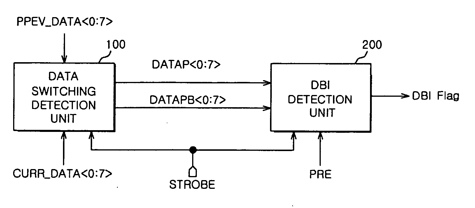
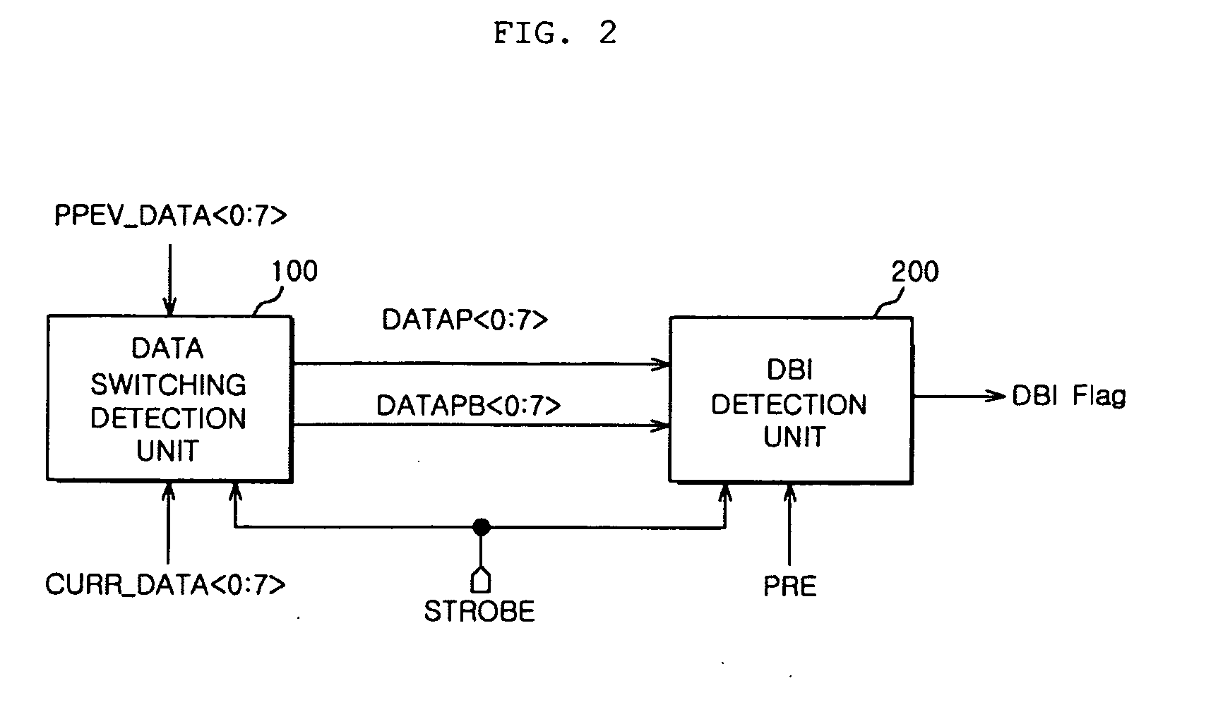
[0028] As shown in FIG. 2, the apparatus for generating a DBI signal in a semiconductor memory apparatus according to the exemplary embodiment of the present invention includes a data switching detection unit 100 that detects whether or not previous data PREV_DATA is consistent with current data CURR_DATA and outputs detection signals DATAP and DATAPB according to the detection result, and a DBI detection unit 200 that outputs a DBI signal (DBI Flag) according to a difference in charge sharing level using the detection signals.

[002...


PUM


Abstract

An apparatus for generating a DBI signal in a semiconductor memory apparatus includes a data switching detection unit that detects whether or not previous data is consistent with current data and outputs a detection signal according to a detection result, and a DBI detection unit that outputs a DBI signal according to a difference in charge sharing level using the detection signal. Therefore, it is possible to minimize current consumption. Further, since there is no effect due to resistance skew of a transistor, an error in DBI signal generation and an error in data transfer accordingly can be prevented. Therefore, it is possible to improve the reliability of a system to which a semiconductor memory apparatus is applied.

Description

BACKGROUND [0001] 1. Technical Field [0002] The present invention relates to a semiconductor memory apparatus, and more particularly, to an apparatus and a method of generating a DBI signal in a semiconductor memory apparatus. [0003] 2. Related Art [0004] A DBI (Data Bus Inversion) system is used in order to prevent a problem, such as simultaneous switching noise or inter symbol interference, that occurs as the number of data bits to be switched increases upon data transmission, that is, as the number of currently switched data bits among the entire data bits becomes larger than the number of previously switched data bits. [0005] In the DBI system, in order to solve the above problem, when the number of switched data bits is half or more of the number of all data bits, a DBI signal (DBI Flag) is enabled, and inverted data is transmitted, instead of original data, thereby reducing the number of switched data bits to half or less. [0006] Hereinafter, the related art will be described ...

Claims


Application Information

Patent Timeline
Patent Type & Authority Applications(United States)
IPC IPC(8): G11C5/06
CPCG11C7/02G11C7/1048G11C7/1051G11C7/1063G11C5/14G11C7/10
Inventor LEE, DONG UK
Owner SK HYNIX INC
Why Eureka
Try Eureka