Polymer Nanosensor Device

Inactive Publication Date: 2007-06-07
PHYSICAL LOGIC
View PDF23 Cites 42 Cited by
  • Summary
  • Abstract
  • Description
  • Claims
  • Application Information

AI Technical Summary

Benefits of technology

[0008] In still other and preferred embodiments of the invention, the particles are electrically conductive nanospheres. The use of conductive nanospheres allows a relatively small perturbation to the array to be measured by electrical continuity across the device. In other embodiments, the particles are nanocrystals or quantum dots whose optical properties depend on the state of coale

Problems solved by technology

The current generation of such sensors needs power, which increases their size and limits the

Method used


Image

  • Polymer Nanosensor Device
  • Polymer Nanosensor Device
  • Polymer Nanosensor Device

Examples


Embodiment Construction

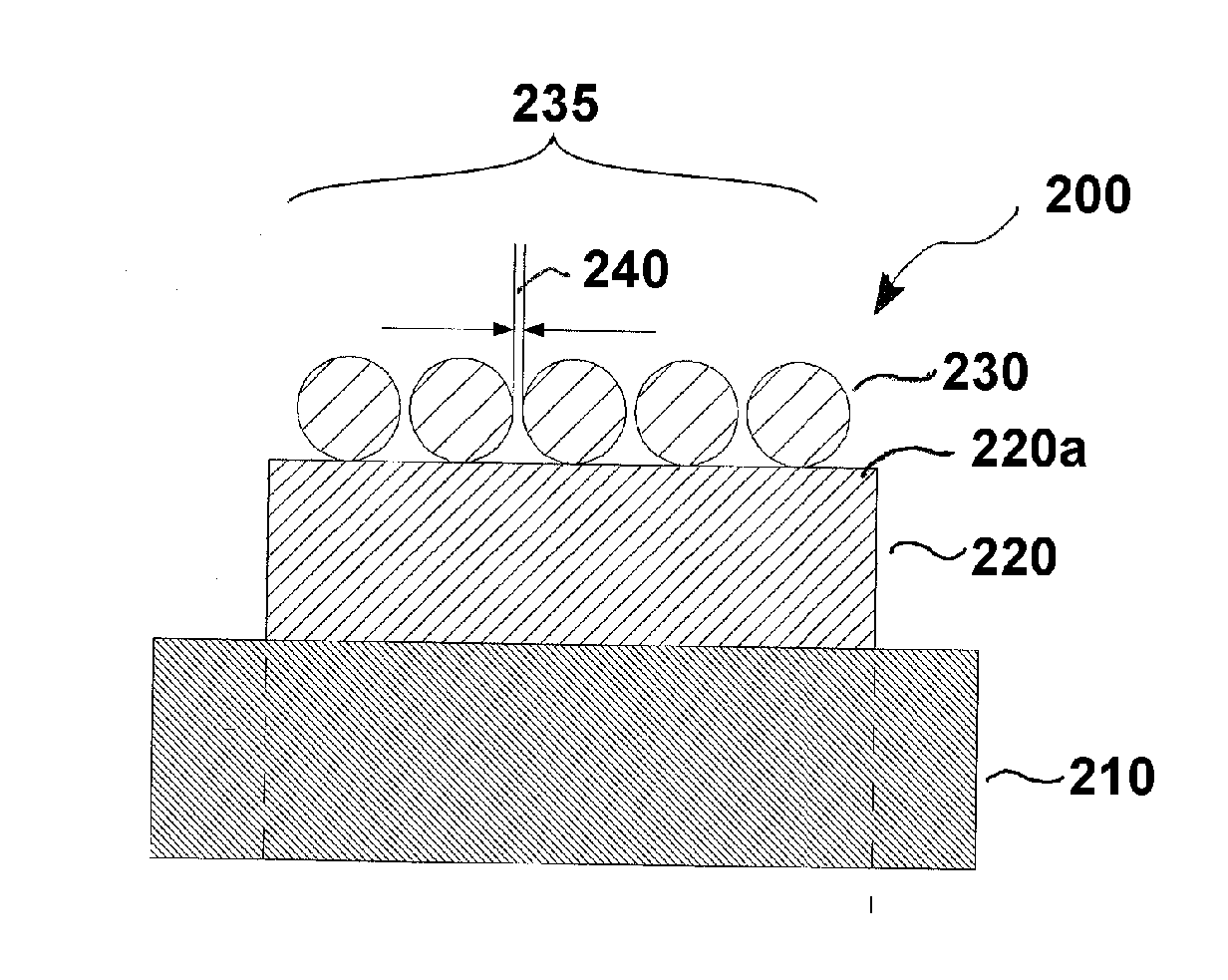
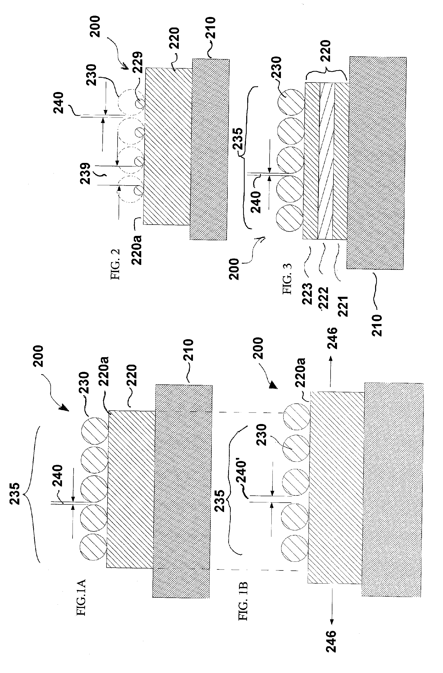
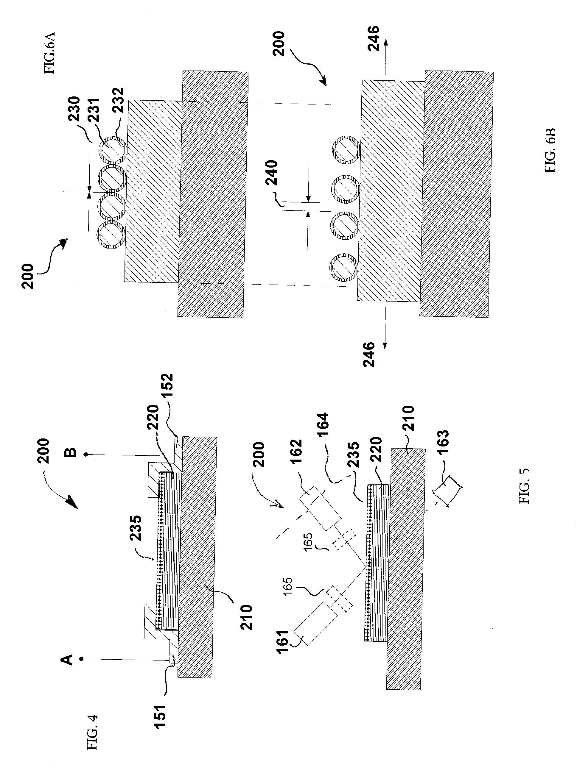
[0019] Referring to FIGS. 1 through 8, wherein like reference numerals refer to like components in the various views, there is illustrated therein a new and improved polymer nanosensor device, generally denominated 200 herein.

[0020] In accordance with the present invention, as illustrated in FIG. 1A a nanoscale device 200 is constructed on a substrate 210. A relatively thin polymeric layer 220 is disposed on substrate 200. Substantially equiaxed particles 230 are attached on the upper or outer surface 220a of polymer layer 220. The particles 230 are deposited on polymer layer 220 to form an array 235 wherein the thickness of polymer layer 220 is of comparable size scale to the particles 230. In the case of conductive particles, there will be electrical continuity across array 235. A gap 240 may exist between particles 230 in array 235. It is believed that a gap of several nanometers between particles will still lead to electrical continuity because electrons can quantum tunnel acro...


PUM


Abstract

A plurality of particles are densely packed as an array on a flexible substrate. As at least a portion of the substrate responds mechanically to an external stimulus, the coated substrate is useful as a sensor device to the extent that the mechanical response produces a separation between particles resulting in a measurable change in the physical properties of the array. Preferably the particles are conductive, spherical and of nano-scale for greater sensitivity. When the array comprises closely packed conductive nano-particles deformation of the substrate disturbs the electrical continuity between the particles resulting in a significant increase in resistivity. The various optical properties of the device may exhibit measurable changes depending on the size and composition of the nano-particles, as well as the means for attaching them to the substrate.

Description

CROSS REFERENCE TO RELATED APPLICATIONS [0001] The present application claims priority to the U.S. provisional application having Ser. No. 60 / 738,927 entitled “Nanoparticle Vibration and Acceleration Sensors”, filed on Nov. 21, 2006 which is incorporated herein by reference. The present application also claims priority to the U.S. provisional application having Ser. No. 60 / 738,793 entitled “Nanoscale Sensor”, filed on Nov. 21, 2006 which is incorporated herein by reference. The present application further claims priority to the U.S. provisional application having Ser. No. 60 / 738,778 entitled “Polymer Nanosensor Device”, filed on Nov. 21, 2006 which is incorporated herein by reference.BACKGROUND OF INVENTION [0002] The present invention relates to a composition of matter useful structures and configurations for forming sensors having an ultra-high sensitivity to acceleration, deformation, vibration and the like physical disturbances. [0003] Prior methods of sensing small mechanical m...

Claims


Application Information

Patent Timeline
IPC IPC(8): G01B7/16
CPCB82Y5/00B82Y15/00B82Y30/00G01H11/06G01N33/54373G01P15/0802G01P15/0894G01P15/12G01P15/123G01P2015/0828
Inventor OFEK, ERANAXELROD, NOELLICHTENSTEIN, AMIRPARDO-YISSAR, VERED
Owner PHYSICAL LOGIC
Why Eureka
Try Eureka