Formation method of semiconductor structure

A semiconductor and plasma technology, applied in the fields of semiconductor devices, semiconductor/solid-state device manufacturing, electrical components, etc., can solve the problems such as the performance of fin-type field effect transistors that needs to be further improved, and the large leakage current.

Active Publication Date: 2019-11-05
SEMICON MFG INT (SHANGHAI) CORP +1
View PDF8 Cites 0 Cited by
  • Summary
  • Abstract
  • Description
  • Claims
  • Application Information

AI Technical Summary

Problems solved by technology

[0004] Fin field effect transistors formed on bulk silicon often have relatively large leakage currents, and the performance of the fin field effect transistors needs to be further improved

Method used


Image

  • Formation method of semiconductor structure
  • Formation method of semiconductor structure
  • Formation method of semiconductor structure

Examples


Embodiment Construction

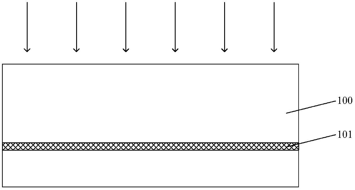
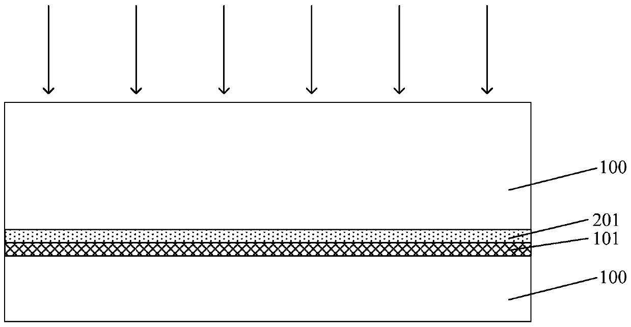
[0032] The structure of the silicon-on-insulator substrate includes: a bottom silicon layer, a buried oxide layer on the surface of the bottom silicon layer, and a top silicon layer on the surface of the buried oxide layer. Forming a semiconductor device on an insulating silicon substrate can effectively reduce the leakage current of the semiconductor device and improve the performance of the semiconductor device.

[0033] Oxygen ions can be implanted into bulk silicon by ion implantation to form a buried oxide layer in bulk silicon, thereby forming a silicon-on-insulator structure, but the ion implanter used for ion implantation usually takes a long time to reach the required level for forming the buried oxide layer. required implant dose, resulting in low efficiency and high cost for forming silicon-on-insulator substrates. In the plasma implantation process, the implantation dose is relatively large, and the implantation dose has nothing to do with the implantation time and...


PUM


Abstract

Provided is a formation method of a semiconductor structure. The method comprises that a semiconductor substrate is provided; a first nitrogen-doped layer is formed in the semiconductor substrate; an oxygen-containing plasma ion implantation technology is used to form an oxygen-doped layer in the surface of the first nitrogen-doped layer, and oxygen-containing plasmas comprise water plasmas at least; a second nitrogen-doped layer is formed on the oxygen-doped layer; and heat treatment is carried out on the semiconductor substrate, so that oxygen atoms in the oxygen-doped layer diffuse into the first and second nitrogen-doped layers to form first and second silicon oxynitride layers. The method can be used to improve performances of the formed semiconductor structure.

Description

technical field [0001] The invention relates to the technical field of semiconductors, in particular to a method for forming a semiconductor structure. Background technique [0002] With the continuous development of semiconductor process technology, process nodes are gradually reduced, and gate-last (gate-last) process has been widely used to obtain an ideal threshold voltage and improve device performance. However, when the feature size of the device is further reduced, even if the gate-last process is adopted, the structure of the conventional MOS field effect transistor can no longer meet the requirements for device performance, and the fin field effect transistor (Fin FET) is obtained as a multi-gate device. received widespread attention. [0003] figure 1 A schematic diagram of a three-dimensional structure of a fin field effect transistor in the prior art is shown. Such as figure 1 As shown, it includes: a semiconductor substrate 10, on which a protruding fin 11 i...

Claims


Application Information

Patent Timeline
Patent Type & Authority Patents(China)
IPC IPC(8): H01L21/02H01L21/336
CPCH01L21/0257H01L29/66803
Inventor 周鸣
Owner SEMICON MFG INT (SHANGHAI) CORP
Why Eureka
Try Eureka