Method for manufacturing angle and curvature detection sensor, and sensor

Active Publication Date: 2018-06-14
IND ACADEMIC COOPERATION FOUND OF SUNCHON NAT UNIV
View PDF0 Cites 0 Cited by
  • Summary
  • Abstract
  • Description
  • Claims
  • Application Information

AI Technical Summary

Problems solved by technology

However, most of currently manufactured physical and chemical sensors are manufactured on a silicone wafer surface in a conventional semiconductor manufacturing process such as etching and deposition, which is difficult to be performed with low costs, large ar

Method used


Image

  • Method for manufacturing angle and curvature detection sensor, and sensor
  • Method for manufacturing angle and curvature detection sensor, and sensor
  • Method for manufacturing angle and curvature detection sensor, and sensor

Examples


Embodiment Construction

[0039]Hereinafter, the constitution and operation of an embodiment of the present invention will be described with reference to the accompanying drawings.

[0040]Note that the same or similar components in the drawings are designated by the same reference numerals as far as possible even if they are shown in different drawings

[0041]Hereinafter, detailed descriptions related to well-known functions or configurations will be ruled out in order not to unnecessarily obscure subject matters of the present invention.

[0042]Furthermore, when it is described that one comprises (or includes or has) some elements, it should be understood that it may comprise (or include or has) only those elements, or it may comprise (or include or have) other elements as well as those elements if there is no specific limitation.

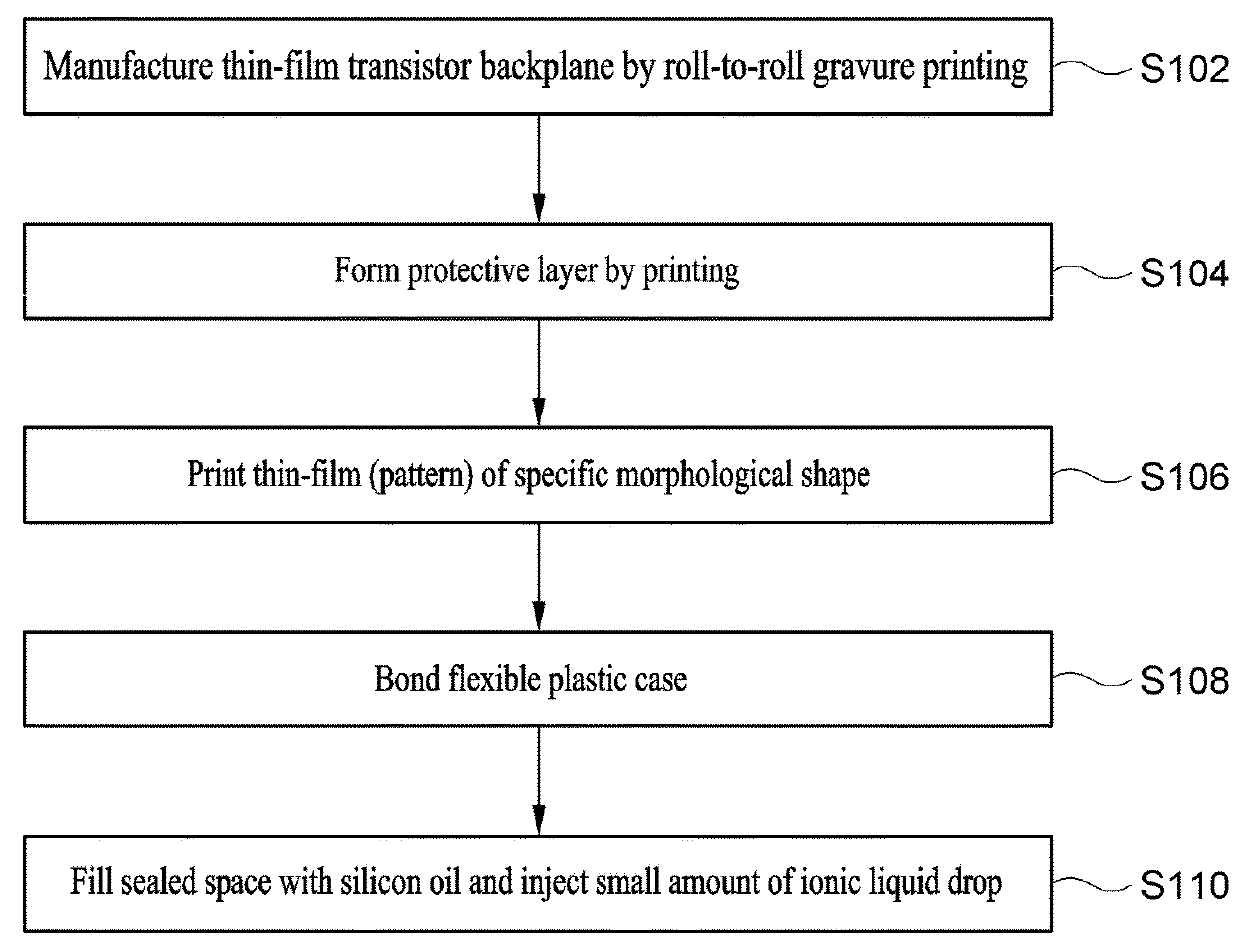
[0043]FIG. 1 is a manufacturing process chart of an angel and curvature detection sensor according to an embodiment of the present invention.

[0044]In operation S102, a thin-film transist...


PUM


Abstract

The present invention relates to a method for manufacturing an angle and curvature detection sensor, and the sensor and, more specifically, to: a method for manufacturing a thin-film transistor array-based backplane by a roll-to-roll gravure printing process and manufacturing a sensor for measuring an angle change and a degree of curvature of the X axis and the Y axis by using the backplane; and the sensor. The method for manufacturing an angle and curvature detection sensor, according to an embodiment of the present invention, comprises the steps of: manufacturing a thin-film transistor backplane by a roll-to-roll gravure printing process; forming a protective layer on the thin-film transistor backplane by printing; forming a sealed space by adhering a flexible plastic case onto the upper part of the protective layer by means of an adhesive; and filling the sealed space with a first liquid and injecting a second liquid.

Description

TECHNICAL FIELD[0001]The present invention relates to a method for manufacturing an angle and curvature detection sensor and the sensor, and more particularly, to a method for manufacturing a thin-film transistor array-based backplane by a roll-to-roll gravure printing process to manufacture a sensor for measuring an angle change and a degree of curvature of a X-axis and a Y-axis by using the backplane and the sensor.BACKGROUND ART[0002]As a material, printing, and process technology applied to printing electronics is developed, researches on manufacturing a printed thin-film transistor backplane capable of integrating a transistor element in an array type over an large area on a flexible board is being actively performed, and various applied devices such as a flexible display, an E-paper, an E-skin that is an expandable circuit, a wall-paper, and a flexible pressure sensor are being manufactured by using the backplane as a type of a sample for demonstration.[0003]Also, due to devel...

Claims


Application Information

Patent Timeline
IPC IPC(8): B41F13/187G01B7/293G01B7/30B41F13/11
CPCB41F13/187G01B7/293G01B7/30B41F13/11B82Y30/00B82Y10/00B82Y15/00H10K19/10
Inventor CHO, GYOU-JINSUN, JUN FENGLEE, WOO KYUNOH, JIN SOO
Owner IND ACADEMIC COOPERATION FOUND OF SUNCHON NAT UNIV
Why Eureka
Try Eureka