Multi-band LC resonance voltage-controlled oscillator with adjustable negative resistance cell

a voltage-controlled oscillator and negative resistance technology, applied in the direction of pulse automatic control, oscillation generator, resonance circuit tuning, etc., can solve the problems of increasing the phase noise of the voltage-controlled oscillator, and the difficulty of integrating a wide-band lc resonance voltage-controlled oscillator in a multi-band multi-mode wireless transceiver, so as to suppress phase noise and suppress noise

Inactive Publication Date: 2007-06-14
ELECTRONICS & TELECOMM RES INST
View PDF13 Cites 29 Cited by
  • Summary
  • Abstract
  • Description
  • Claims
  • Application Information

AI Technical Summary

Benefits of technology

[0011] Also, the present invention is directed to a wide-band LC resonance voltage-controlled oscillator, which suppresses phase noise caused by a tail current source that is adopted for controlling fluctuation in oscil...

Problems solved by technology

It is difficult to embody a wide-band LC resonance voltage-controlled oscillator in a multi-band multi-mode wireless transceiver.
However, the tail ...

Method used


Image

  • Multi-band LC resonance voltage-controlled oscillator with adjustable negative resistance cell
  • Multi-band LC resonance voltage-controlled oscillator with adjustable negative resistance cell
  • Multi-band LC resonance voltage-controlled oscillator with adjustable negative resistance cell

Examples


exemplary embodiment 1

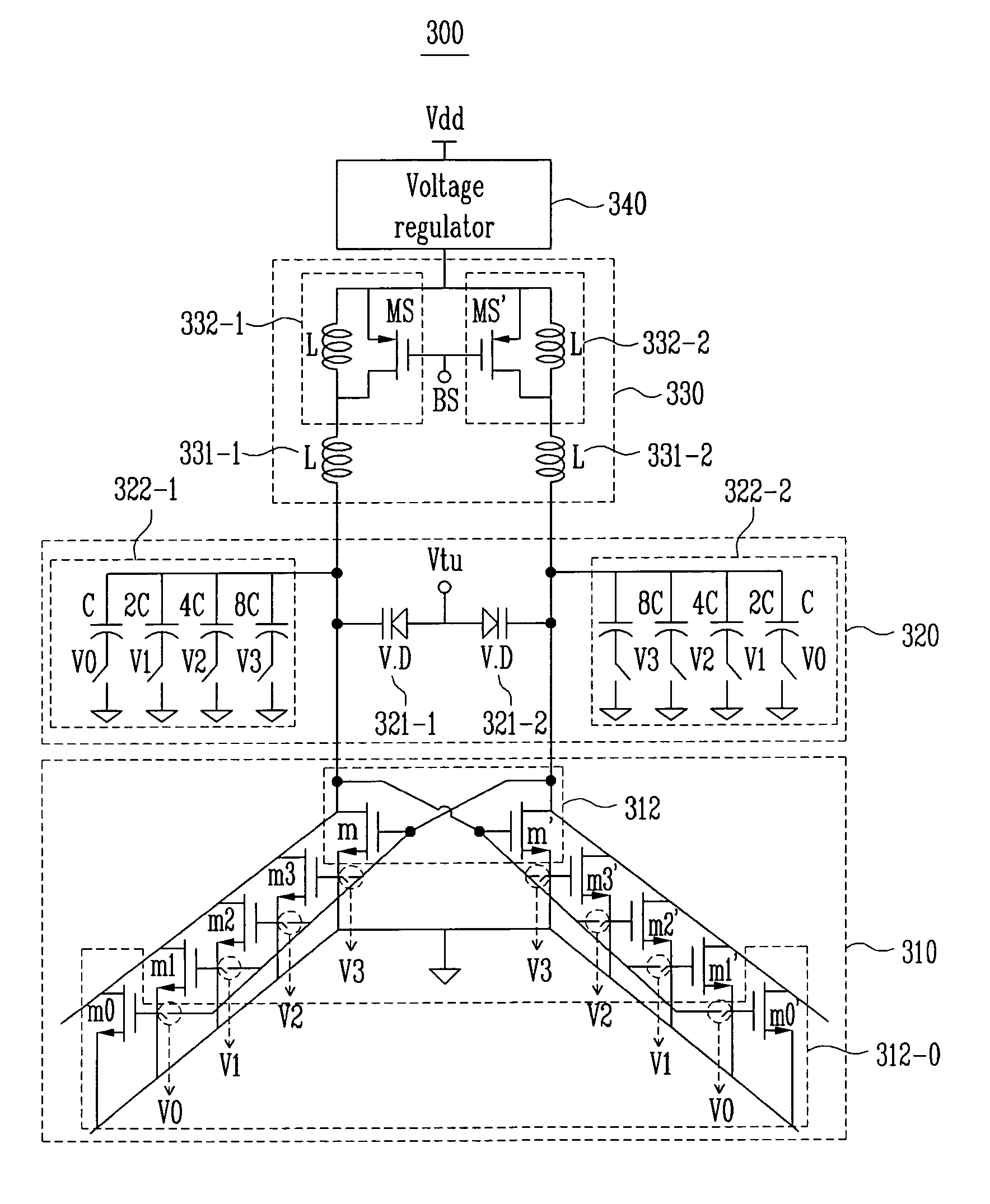
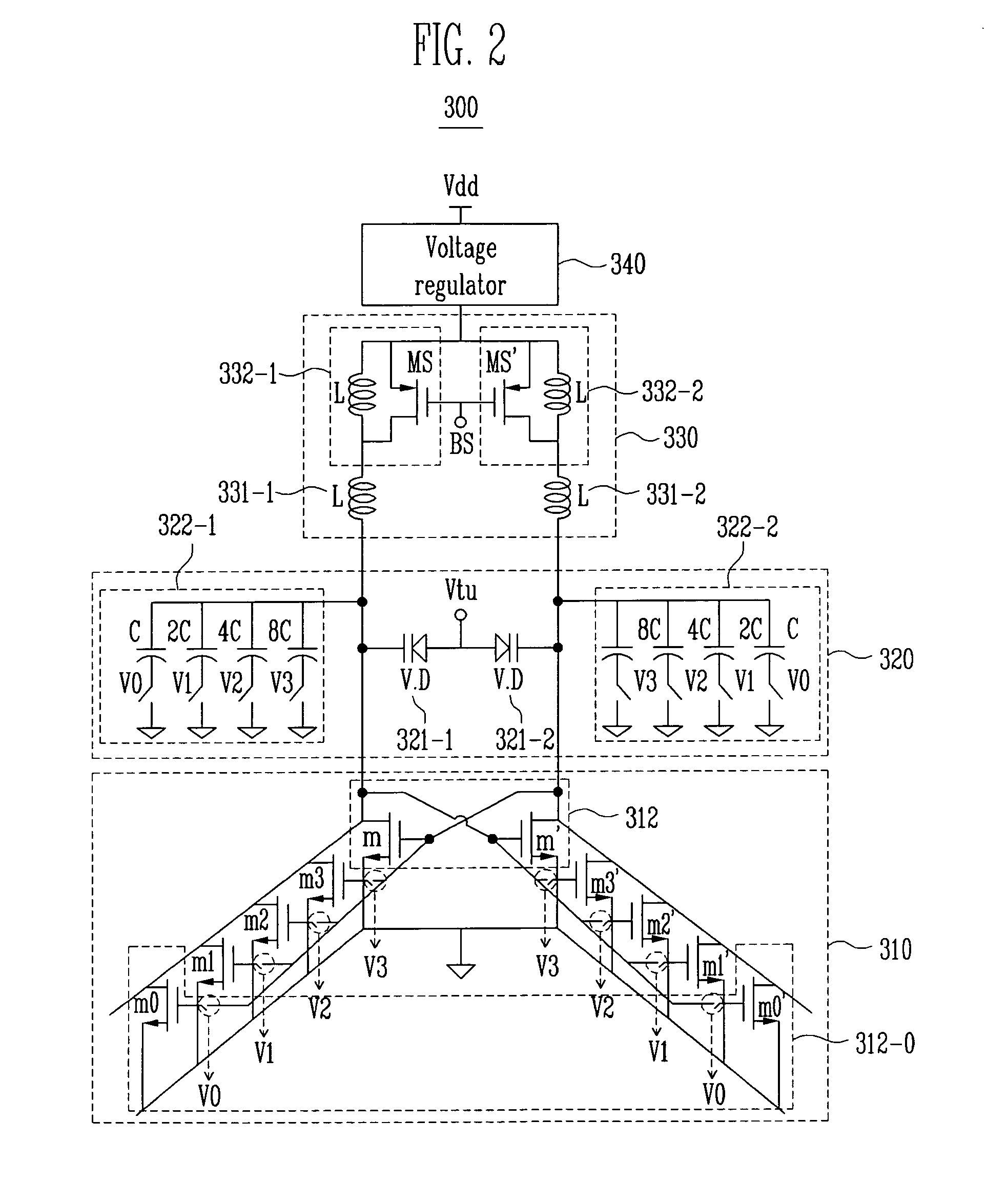
[0024]FIG. 2 is a circuit diagram of a wide-band LC resonance voltage-controlled oscillator 300 according to an exemplary embodiment of the present invention.

[0025] Referring to FIG. 2, the LC resonance voltage-controlled oscillator 300 includes an inductor 330, a capacitor 320, a discrete negative resistance cell 310, and a voltage regulator 340. Specifically, the inductor 330 provides an inductance element and the capacitor 320 provides a capacitance element that together determine the frequency of an oscillation wave. The discrete negative resistance cell 310 provides a discretely determined negative resistance element to keep the amplitude of the oscillation wave constant. Also, the voltage regulator 340 keeps a voltage applied from a power supply voltage terminal to the inductor 330 constant.

[0026] The inductor 330 includes a first inductor 332-1 and 331-1 and a second inductor 332-2 and 331-2, which are connected to the voltage regulator 340 and have different current paths....

exemplary embodiment 2

[0041]FIG. 4 is a circuit diagram of a wide-band LC resonance voltage-controlled oscillator 301 including an emitter-degeneration coupled pair 352 in addition to a negative resistance cell 350 according to another exemplary embodiment of the present invention.

[0042] Referring to FIG. 4, the LC resonance voltage-controlled oscillator 301 includes a voltage regulator 340, an inductor 330, first and second discrete capacitors 322-1 and 322-2, and first and second varactors 321-1 and 321-2, which perform almost the same functions as those of FIG. 2. A first inductor 332-1 and 331-1, the first discrete capacitor bank 322-1, and the first varactor 321-1 form one LC oscillation path, while a second inductor 332-2 and 331-2, the second discrete capacitor bank 322-2, and the second varactor 321-2 form the other LC oscillation path.

[0043] In the present exemplary embodiment, the LC resonance voltage-controlled oscillator 301 is structurally characterized by the emitter-degeneration coupled ...

exemplary embodiment 3

[0048]FIG. 5 is a circuit diagram of a wide-band LC resonance voltage-controlled oscillator 302 with an adjustable emitter-degeneration negative resistance cell 360 according to still another exemplary embodiment of the present invention.

[0049] Referring to FIG. 5, the negative resistance cell 360 includes a plurality of unit discrete negative resistance cells that are connected in parallel in response to control bit signals V0˜V3. Each of the unit discrete negative resistance cells 362-0 is comprised of a pair of unit MOS transistors m, m′, m0, m0′, ˜m3, and m3′, a unit resistor, and a unit capacitor. The pair of unit MOS transistors m, m′, m0, m0′, ˜m3, and m3′ are configured as an emitter-degeneration coupled pair in which one drain is connected to the other source, and have drains connected to a connection node between an inductor and a discrete capacitor bank. The unit resistor is connected in series to the pair of unit MOS transistors m, m′, m0, m0′, ˜m3, and m3′, and the uni...


PUM


Abstract

Provided is an LC resonance voltage-controlled oscillator (VCO) used for a multi-band multi-mode wireless transceiver. In order to generate a multi-band frequency, a capacitor bank and a switchable inductor are included in the LC resonance voltage-controlled oscillator. The LC resonance voltage-controlled oscillator employs an adjustable emitter-degeneration negative resistance cell in place of tail current sources in order to compensate for non-uniform oscillation amplitude caused by the capacitor bank and prevent the degradation of a phase noise due to the tail current sources. The LC resonance voltage-controlled oscillator includes an inductor providing an inductance element partially determining the frequency of an oscillation wave; a discrete capacitor bank providing a capacitance element partially determining the frequency of the oscillation wave and being discretely determined by a control bit signal; and a discrete negative resistance cell providing a negative resistance element that is discretely determined by the control bit signal, to keep the amplitude of the oscillation wave constant.

Description

CROSS-REFERENCE TO RELATED APPLICATION [0001] This application claims priority to and the benefit of Korean Patent Application Nos. 2005-119516, filed Dec. 8, 2006, and 2006-55270, filed Jun. 20, 2006, the disclosures of which are incorporated herein by reference in their entirety. BACKGROUND [0002] 1. Field of the Invention [0003] The present invention relates to a multi-band inductor-capacitor (LC) resonance voltage-controlled oscillator (VCO) and, more specifically, to a multi-band LC resonance voltage-controlled oscillator that operates in a multi-band multi-mode and compensates for fluctuation in the amplitude of an oscillation wave. [0004] 2. Discussion of Related Art [0005] It is difficult to embody a wide-band LC resonance voltage-controlled oscillator in a multi-band multi-mode wireless transceiver. [0006] Nowadays, capacitor banks 122-1 and 122-2 and varactors 121 are mounted in an LC resonance portion with a fixed inductor 130 as shown in FIG. 1, in order to extend the fr...

Claims


Application Information

Patent Timeline
IPC IPC(8): H03B5/08
CPCH03B2201/0208H03B2201/0266H03J2200/10H03B5/1228H03B5/1215H03B5/1243H03B5/1265H03B5/1271H03B5/08
Inventor LEE, JA YOLKIM, KWI DONGKWON, CHONG KIKIM, JONG DAELEE, SANG HEUNGCHO, KYOUNG IK
Owner ELECTRONICS & TELECOMM RES INST
Why Eureka
Try Eureka