
Method for fabricating semiconductor device

a semiconductor and device technology, applied in the field of semiconductor device fabrication, can solve the problems of difficult height difference between active region and field region, and the inability to perform lpc opening process and gap filling process,

Inactive Publication Date: 2007-06-14
SK HYNIX INC
View PDF3 Cites 1 Cited by
  • Summary
  • Abstract
  • Description
  • Claims
  • Application Information

AI Technical Summary

Benefits of technology

[0016] It is, therefore, an object of the present invention to provide a method for fabricating a semiconductor device, wherein the method reduces a self-aligned contact fail of a landing plug contact.

Problems solved by technology

Accordingly, it may be difficult to perform a LPC opening process and a gap-filling process.
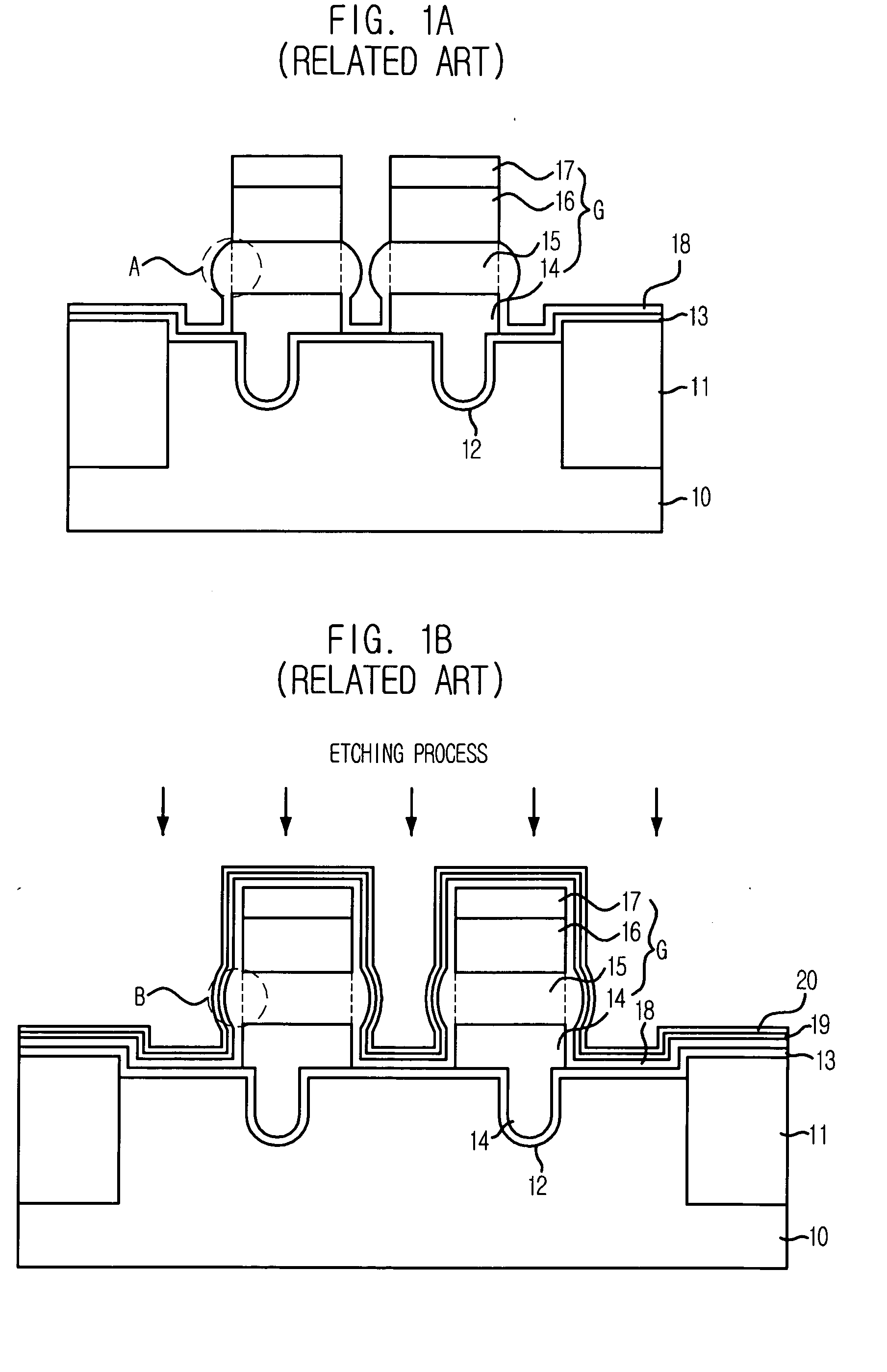
Particularly, in case of the DRAM devices, there may be a height difference between an active region and a field region when a recess gate is used to improve a refresh property.
The difference in the stress of the silicide layer causes an excessive oxidation on sidewalls of the silicide layer and thus, a self-aligned contact (SAC) fail may often be induced.
As described above, after performing a light oxidation process, an abnormal oxidation may occur in the tungsten silicide layer because the tungsten silicide layer has different levels of stress caused by a height difference between the recess gate and the device isolation structure.
Afterwards, sidewalls of the tungsten silicide layer are more likely to be damaged during the landing plug contact (LPC) process.
Also, the abnormal oxidation may take place by a reaction between silicon atoms of the tungsten silicide layer and oxygen gas used for the light oxidation process.

Method used


Image

  • Method for fabricating semiconductor device
  • Method for fabricating semiconductor device
  • Method for fabricating semiconductor device

Examples


Embodiment Construction

[0022] Hereinafter, detailed descriptions on certain embodiments of the present invention will be provided with reference to the accompanying drawings.

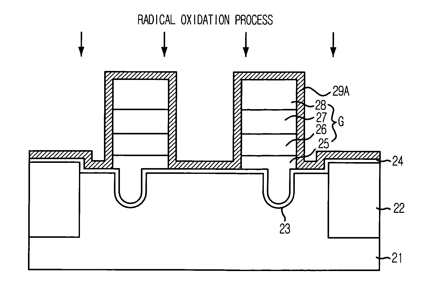
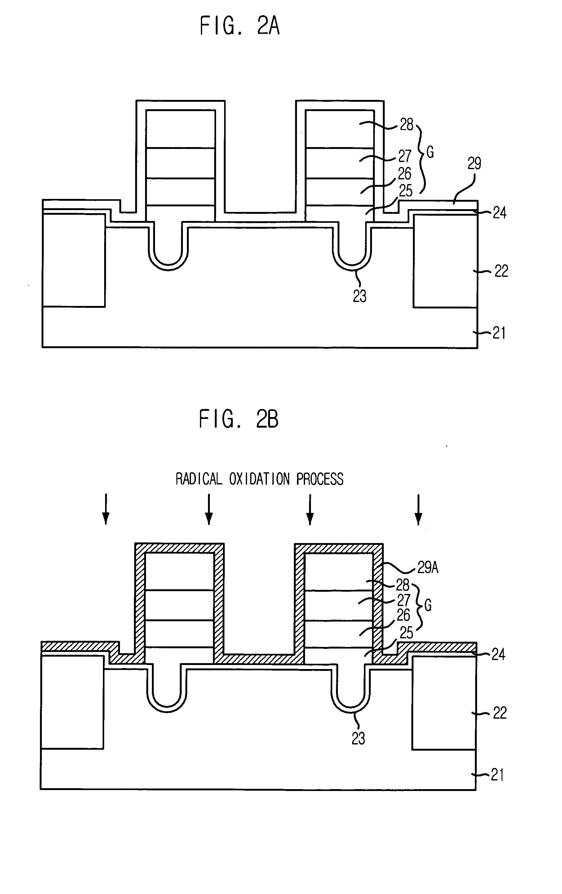
[0023]FIGS. 2A to 2C are cross-sectional views illustrating a method for fabricating a semiconductor device in accordance with an embodiment of the present invention.

[0024] As shown in FIG. 2A, a plurality of device isolation layers 22 are formed in certain portions of a substrate 21 through a shallow trench isolation (STI) process. Then, a plurality of recesses 23 are formed in predetermined portions of the substrate 21.

[0025] A gate insulation layer 24 is formed over the above resulting structure and afterwards, a plurality of recess gate lines G are formed over the gate insulation layer 24 being partially filled into the recesses 23. Each of the recess gate lines G is formed by sequentially stacking the gate insulation layer 24, a polysilicon layer 25, a tungsten silicide layer 26, a gate hard mask 27, and an anti-reflective coa...


PUM

PropertyMeasurementUnit
temperatureaaaaaaaaaa
pressureaaaaaaaaaa

Abstract

A method for fabricating a semiconductor device includes: providing a substrate structure in which a plurality of gate lines are already formed; forming a capping layer over the substrate structure; oxidizing the capping layer; and forming an insulation layer over the oxidized capping layer. The capping layer may include a nitride-based material. The insulation layer may include substantially the same material as the capping layer. The oxidizing of the capping layer may comprise performing a radical oxidation process.

Description

FIELD OF THE INVENTION [0001] The present invention relates to a method for fabricating a semiconductor device; and more particularly, to a method for fabricating a semiconductor device to reduce a self-aligned contact failure of a landing plug contact. DESCRIPTION OF RELATED ARTS [0002] In a landing plug contact (LPC) module process of dynamic random access memory (DRAM) devices with a size of approximately 80 nm or lower, although the size of the devices has been reduced, a thickness of a gate spacer has not been decreased. Accordingly, it may be difficult to perform a LPC opening process and a gap-filling process. [0003] Particularly, in case of the DRAM devices, there may be a height difference between an active region and a field region when a recess gate is used to improve a refresh property. As a result, a difference in a stress of a silicide layer which forms a gate pattern may be generated. The difference in the stress of the silicide layer causes an excessive oxidation on ...

Claims


Application Information

Patent Timeline
Patent Type & Authority Applications(United States)
IPC IPC(8): H01L21/471
CPCH01L21/28114H01L21/28247H01L21/76826H01L21/76828H01L21/76829H01L29/42376H01L29/66621H01L21/18H01L21/283H01L21/31H10B99/00
Inventor NAM
Owner SK HYNIX INC
Learn More