A method for manufacturing a three-dimensional memory device and its device structure

A technology for three-dimensional storage and manufacturing methods, applied in the direction of semiconductor devices, electrical solid devices, electrical components, etc., can solve the problems of electrical connection failure, distorted photolithography process pattern, contact holes cannot fall on the steps correctly, etc., to reduce Effects of deformation and distortion, increasing effective contact area, reducing contact failure problems

Active Publication Date: 2019-01-01
YANGTZE MEMORY TECH CO LTD
View PDF4 Cites 0 Cited by
  • Summary
  • Abstract
  • Description
  • Claims
  • Application Information

AI Technical Summary

Problems solved by technology

[0006] However, in the subsequent step etching process, the independent partition steps will be deformed to a certain extent, such as Figure 4-5 As shown, the end of the independent partition pattern step (SSDS) away from the core region (Core) of the storage device is enlarged and deformed due to the cumulative etching process, which makes the original rectangular step pattern design become after the cumulative etching process Oblique trapezoidal figure, which affects the implementation of the later electrical connection contact hole process
like Image 6 As shown, since the step is formed after the cumulative etching process, the step width on the side close to the core area is narrow, and the step width on the side away from the core area is wide, so that a part of the contact hole pattern on the edge is in the The narrow step area part cannot realize the opening operation of lithography and etching, even the wider step area away from the core area, because the step width is still uneven, resulting in a part of the contact hole pattern cannot be completely completed. Realize lithography and etching opening operations
This situation causes the gates of the memory cells of some three-dimensional memory devices to fail to effectively form a contact hole electrically connected to it, and forms an invalid contact hole (Fail Contact), thereby affecting the normal operation of the device.
[0007] In addition, if Figure 7 As shown, in the process of forming the pattern of the core area (Core) and SSDS, due to the closeness of the photoresist to each other, there will be certain interference problems, and the pattern will be distorted in the photolithography process: in the subsequent etching process , this distortion will be brought to the back step, and finally the contact hole cannot fall on the step correctly, forming an invalid contact hole (Fail Contact), resulting in the failure of the electrical connection
[0008] In summary, when the structure of the three-dimensional memory device becomes more and more complex, the number of step layers increases, and the steps change from one-way distribution to two-way distribution, the previous etching process of the core area and the step area cannot meet its pattern. Due to the various deformations of the step pattern in the etching process, the subsequent process of forming contact holes cannot be correctly implemented on each step region
There is currently no effective solution to this problem, which seriously restricts the further development of 3D memory devices.

Method used


Image

  • A method for manufacturing a three-dimensional memory device and its device structure
  • A method for manufacturing a three-dimensional memory device and its device structure
  • A method for manufacturing a three-dimensional memory device and its device structure

Examples


Embodiment 1

[0055] refer to Figure 8 As shown, Embodiment 1 of the present invention proposes a method for manufacturing a three-dimensional memory device, including the following steps:

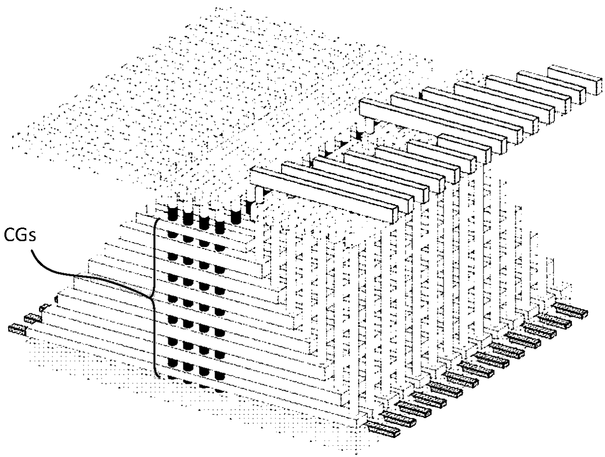
[0056] A substrate is provided, on which a three-dimensional memory device area is formed, and the three-dimensional memory device area includes a multi-layer memory stack structure sequentially formed on the substrate;

[0057] forming a core platform area and a plurality of partition pattern areas adjacent to at least one side of the core platform area by forming the stacked structure through lithography and etching processes;

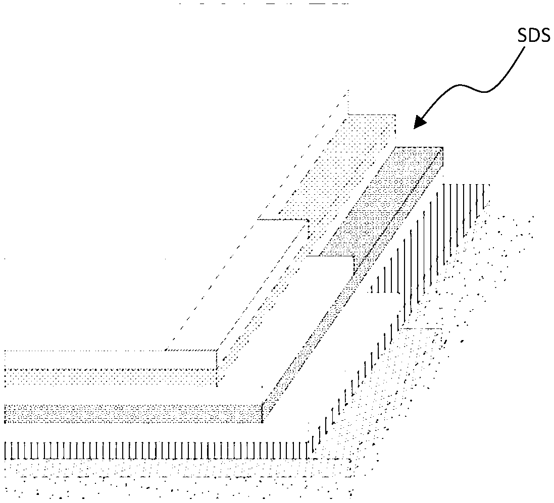
[0058] Each of the plurality of partitioned pattern areas is formed as a trapezoidal three-dimensional structure 1, and at a cross-section in a direction parallel to the side of the core platform area and perpendicular to the surface of the substrate, a base is longer than The isosceles trapezoid of the top side, and, from the section 11 closest to the core platform area to ...

Embodiment 2

[0061] refer to Figure 9 As shown, Embodiment 2 of the present invention proposes a method for manufacturing a three-dimensional memory device, including the following steps:

[0062] A substrate is provided, on which a three-dimensional memory device area is formed, and the three-dimensional memory device area includes a multi-layer memory stack structure sequentially formed on the substrate;

[0063] forming a core platform area and a plurality of partition pattern areas adjacent to at least one side of the core platform area by forming the stacked structure through lithography and etching processes;

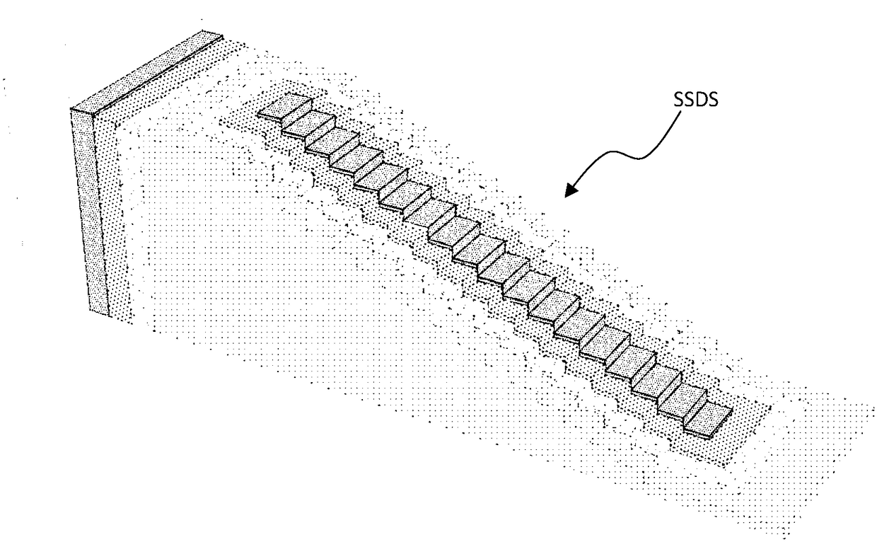
[0064] Each of the plurality of partitioned graphics areas 2 includes: a first rectangular area 21 located on the side away from the core platform area, a second rectangular area 22 close to the side of the core platform area, and An isosceles trapezoidal area 23 located between the first rectangular area 21 and the second rectangular area 22, wherein the long side length of...

Embodiment 3

[0067] The third embodiment is a further improvement on the second embodiment above, and the same parts as the second embodiment will not be repeated.

[0068] Such as Figure 10 As shown, the isosceles trapezoidal area 23 is composed of a plurality of sub-rectangular areas 231 of different lengths, and the length of each of the sub-rectangular areas 231 is from the second rectangular area 22 to the first rectangular area 21 The direction of is gradually reduced, and the length relationship between every two adjacent sub-rectangular areas 231 is:

[0069] b=a+2*TKss / n,

[0070] Wherein: b is the length of the sub-rectangular area closer to the second rectangular area in the two adjacent sub-rectangular areas, a is the length of the sub-rectangular area closer to the first rectangular area in the two adjacent sub-rectangular areas, and TKss is the described The total height of the step structure, n is the number of steps of the step structure, wherein the value range of n is ...


PUM


Abstract

The invention provides a manufacturing method of a three-dimensional memory device and a device structure thereof. By optimizing the graphic design of a staircase divide scheme, the influence of lithography and etching processes on the graphical deformation and distortion of the staircase divide scheme is reduced, the effective contact area of the stair region is substantially increased, and the contact failure of the electrical connecting lines of 3D NAND is reduced.

Description

technical field [0001] The invention relates to the field of semiconductor devices and their manufacture, in particular to a manufacturing method of a three-dimensional flash storage device and its device structure. Background technique [0002] With the continuous improvement of market demand for memory capacity, the number of memory cells that can be provided per unit area by traditional memory based on planar or two-dimensional structures is approaching the limit, which cannot further meet the market demand for larger capacity memory. Just like several bungalows built on a limited plane, these bungalows are neatly arranged, but as the demand continues to increase, the number of bungalows continues to blow out, but in the end this limited plane can only accommodate a certain number of bungalows. Cannot continue to increase. In particular, planar flash memory (NAND) is approaching its practical expansion limit, which brings severe challenges to the semiconductor memory ind...

Claims


Application Information

Patent Timeline
Patent Type & Authority Patents(China)
IPC IPC(8): H01L27/11578
Inventor 华文宇李思晢洪培真骆中伟夏志良霍宗亮
Owner YANGTZE MEMORY TECH CO LTD
Why Eureka
Try Eureka