Paste Coater and PoP Automatic Mounting Apparatus Employing the Same

a technology of automatic mounting and paste coater, which is applied in the direction of soldering apparatus, manufacturing tools,auxillary welding devices, etc., can solve the problems of difficult adjustment or maintenance of the rotatory flatness of the rotary disc, non-comparable height of the ball electrode, and inability to achieve uniform volume of transferred solder paste for all ball electrodes, etc., to achieve efficient stacking and packaging

Inactive Publication Date: 2007-06-21
IBM CORP
View PDF4 Cites 8 Cited by
  • Summary
  • Abstract
  • Description
  • Claims
  • Application Information

AI Technical Summary

Benefits of technology

[0008] One objective of the present invention is to provide a paste coater that can apply a satisfactory amount of a solder paste to small-diameter bump (i.e. ball, stud, etc.) electrodes arranged at small pitches, and a PoP automatic mounting apparatus that employs this paste coater.
[0010] Since the gap adjustment mechanism can precisely adjust the film thickness of the solder paste applied to the transfer roller, the paste coater can apply a satisfactory amount of solder paste on small-diameter bump electrodes arranged at a small pitch.
[0014] Since the PoP automatic mounting apparatus applies solder paste to the bump electrodes of the second semiconductor package and then mounts the second semiconductor package on the first, the two semiconductor packages can be efficiently stacked and packaged.

Problems solved by technology

However, with this method, it is difficult to adjust or maintain the rotatory flatness of the rotary disc, and since the rotatory flatness varies each time the disc is detached, uniform volume of the transferred solder paste is not available for all the ball electrodes.
This problem is especially seen in warped semiconductor packages, resulting in non uniform ball electrode heights leading to coating discrepancies occurring during the spreading of the solder paste.
Another problem occurs when the ball electrodes are dipped to half their height leading to bridges forming between the electrodes.
However, this method is difficult to perform where a wiring pattern has a pitch of 0.3 mm or smaller.
Further, since this method does not allow for the coating of too much solder paste, one is unable to absorb the non uniform height of a warped semiconductor package with excess solder paste.
In addition, it is difficult to utilize this method with a module where an SMC (Surface Mount Component) is mounted, especially a PoP module that requires the application of a solder paste to a wiring pattern on a component mounting side.
By using a combined method in which both the disc squeegee and the paste screen printing method are used, the amount of solder paste applied can be increased, however a increase in costs can not be avoided.

Method used


Image

  • Paste Coater and PoP Automatic Mounting Apparatus Employing the Same
  • Paste Coater and PoP Automatic Mounting Apparatus Employing the Same
  • Paste Coater and PoP Automatic Mounting Apparatus Employing the Same

Examples


Embodiment Construction

[0023] The preferred embodiment of the present invention will now be described in detail while referring to the drawings. The same reference numerals are employed to denote identical or corresponding sections, and an explanation for them will not be repeated.

PoP Automatic Mounting Apparatus

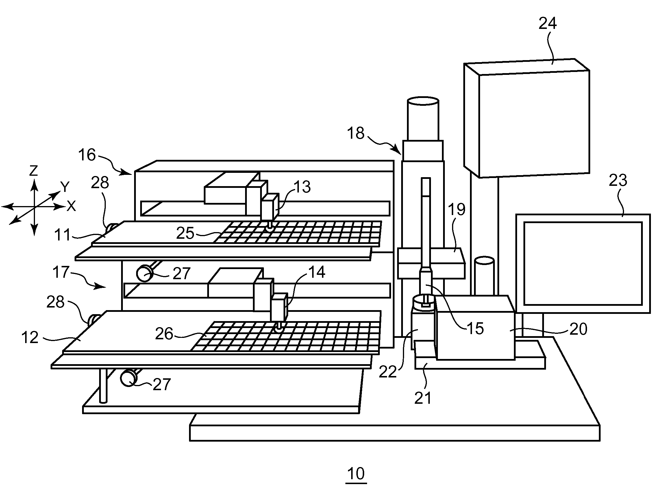
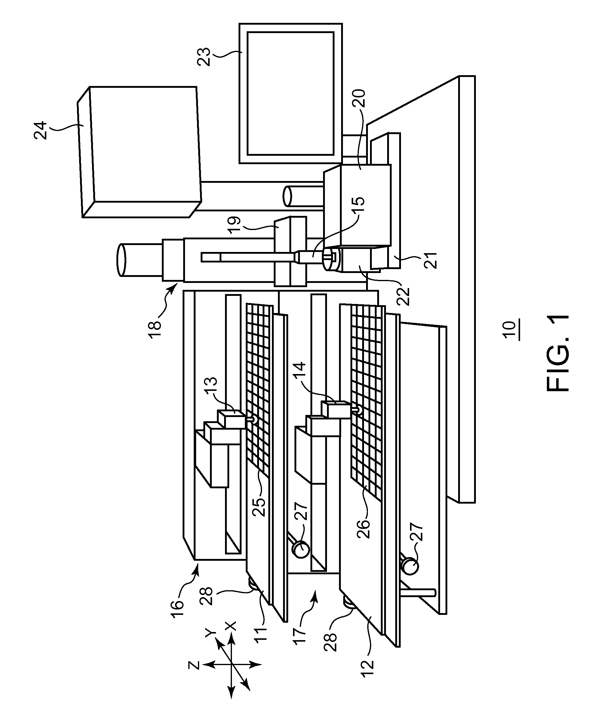
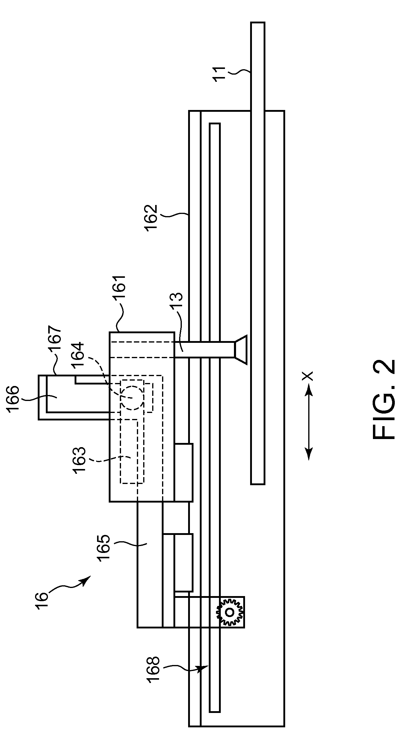
[0024] While referring to FIG. 1, a PoP automatic mounting apparatus 10 according to this embodiment mounts a semiconductor package (i.e. BGA (ball grid arrary), CSP (chip scale packaging) or a flip chip), atop another semiconductor package, and includes: an upper tray 11, a lower tray 12, suction nozzles 13-15, nozzle convey mechanisms 16-18, a position correction unit 19, a paste coater (including a slide mechanism) 20, an inverting extraction unit 21, a positioning illumination and vertically identical viewing camera optical system 22, an alignment color monitor 23 and a controller 24.

[0025] A plurality of upper semiconductor packages 25 are arranged on the upper tray 11, and a plurality of ...


PUM

PropertyMeasurementUnit
diameteraaaaaaaaaa
heightsaaaaaaaaaa
thicknessaaaaaaaaaa

Abstract

A paste coater that can apply an amount of a solder paste to small-diameter bump electrodes at a narrow pitch is described. A paste coater includes: a transfer roller, supported by a sub frame; a roller drive mechanism for rotating the transfer roller; a paste storage unit for storing paste to be supplied to the surface of the transfer roller; a squeegee having a distal edge, parallel to the rotary shaft of the transfer roller, separated by a gap from the distal edge to the surface of the transfer roller; a squeegee holder for holding and including biasing means for pushing the squeegee in a first direction thereby widening the gap; and a gap adjustment mechanism with biasing means for pushing the squeegee in a second direction thereby narrowing the gap.

Description

FIELD OF THE INVENTION [0001] The present invention relates to a paste coater and to a PoP (Package on Package) automatic mounting apparatus that employs the paste coater. More particularly, the present invention relates to a paste coater that applies a solder paste to ball electrodes of a semiconductor package(i.e. ball grid array (BGA)), a chip scale package and flip chip, and a PoP automatic mounting apparatus that mounts one semiconductor package atop another. BACKGROUND OF THE INVENTION [0002] A semiconductor package, such as a BGA, includes an array of multiple projecting ball electrodes. In order to mount a semiconductor package on the obverse face of a printed wiring board, multiple methods are conventionally utilized such as: a disc squeegee method, a paste screen print method, or a combination of the two. These methods generally apply a solder paste to either the ball electrodes of the semiconductor package or to the wiring pattern of the printed wiring board. [0003] The d...

Claims


Application Information

Patent Timeline
Patent Type & Authority Applications(United States)
IPC IPC(8): B05C1/06B05C11/00
CPCH01L24/11H01L24/75H01L2224/13099H01L2224/75H01L2224/7515H01L2224/758H01L2924/01013H01L2924/01015H01L2924/01033H01L2924/01075H01L2924/01082H01L2924/3025H05K3/1275H05K3/3484H05K2201/035H05K2201/10734H05K2203/0139H05K2203/0143H05K2203/0534H01L2924/01005H01L2924/01006H01L2924/014H01L2224/136H01L2224/11822H05K3/3485
Inventor KIMURA, HIDEOYOKOUE, TOSHIYUKISHIOTA, YASUHIKO
Owner IBM CORP
Why Eureka
Try Eureka