Method for controlling polishing process

a polishing process and polishing technology, applied in semiconductor devices, solid-state devices, semiconductor/solid-state device testing/measurement, etc., can solve the problems of copper remaining on the edge of the wafer, over polishing, and dishing around the center of the wafer, so as to increase the uniformity of the thin film layer

Active Publication Date: 2007-06-21
UNITED MICROELECTRONICS CORP
View PDF5 Cites 7 Cited by
  • Summary
  • Abstract
  • Description
  • Claims
  • Application Information

AI Technical Summary

Benefits of technology

[0007] Accordingly, at least one objective of the present invention is to provide a method for controlling a polishing process capable of increasing the uniformity of the thin film layer after the polishing process is performed.
[0008] At least another objective of the present invention is to provide a method of manufacturing a dual damascene capable of improve the uniformity of the electrical properties of the dual damascene structures over the entire wafer.
[0025] In the present invention, the parameters for performing the polishing process are controlled according to the film average thickness distribution of the thin film. Therefore, the problems of copper remaining on the wafer edge, over polishing and dishing can be overcome. Further, the electrical properties of the dual damascene structures are uniform to each other over the entire wafer. Additionally, the film average thickness distribution of the prior wafer and the removal rate recipe used in the prior polish run on the prior wafer are used to estimate the current film average thickness distribution and the current removal rate recipe. Therefore, the electrical properties of the dual damascene structures on the different wafers are uniform.

Problems solved by technology

However, the polishing result of the chemical mechanical polishing process is also affected by the factors other than the process parameters.
Hence, the yield and the reliability of the polishing process are affected.
Accordingly, after the chemical mechanical polishing process is performed, the problems of copper remaining on the wafer edge and over polishing and dishing around the center of the wafer happen.

Method used


Image

  • Method for controlling polishing process
  • Method for controlling polishing process
  • Method for controlling polishing process

Examples


Embodiment Construction

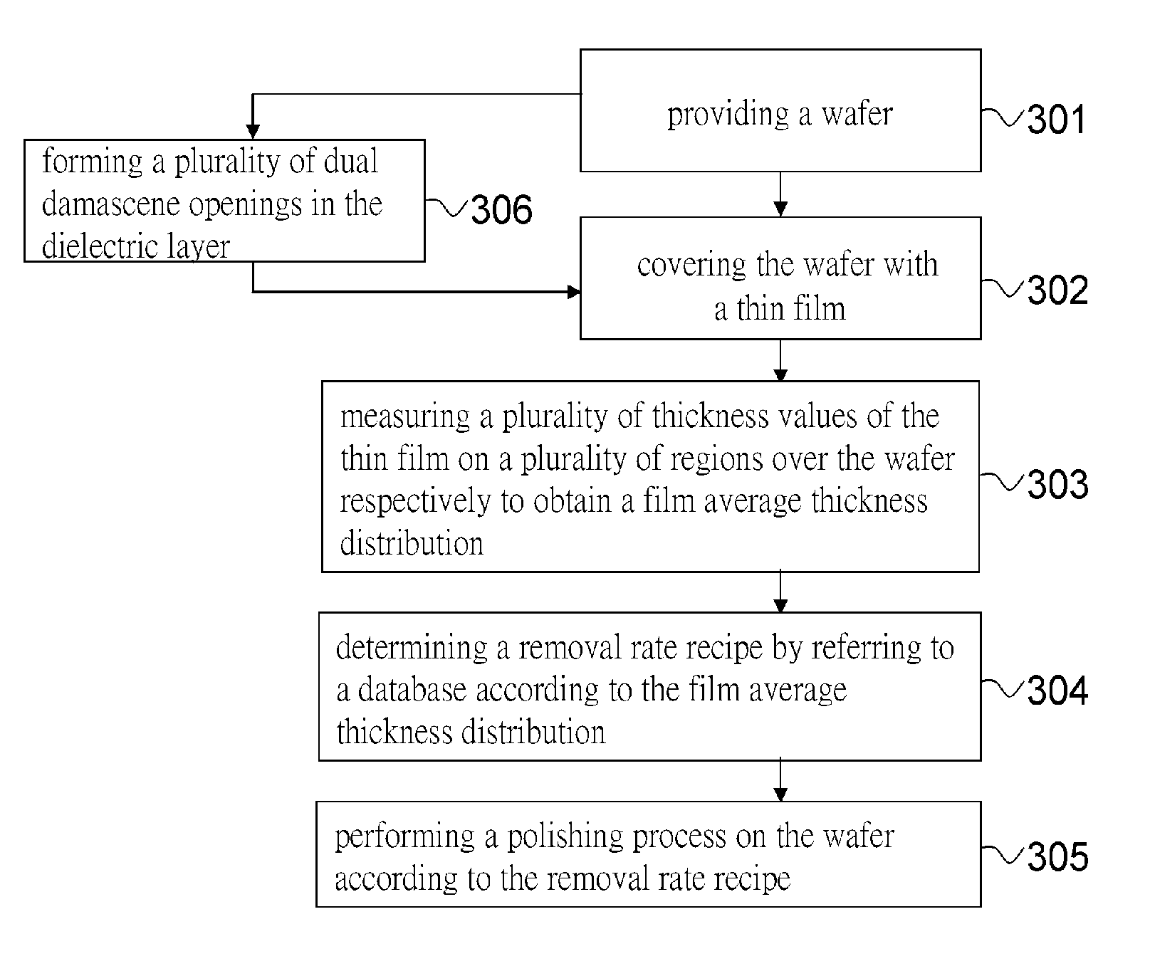
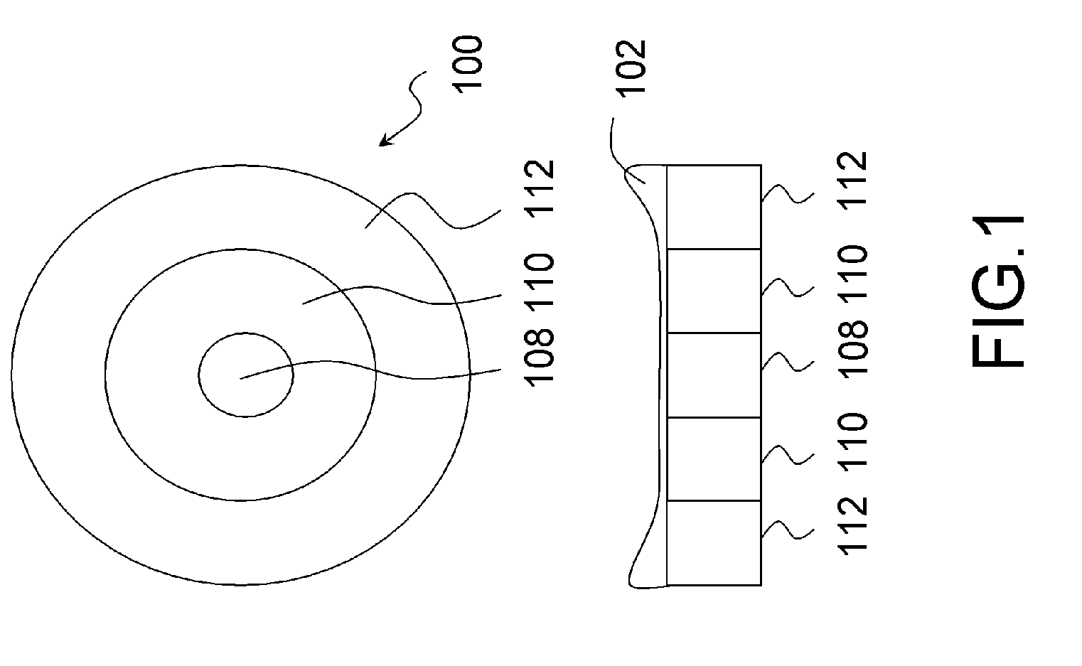
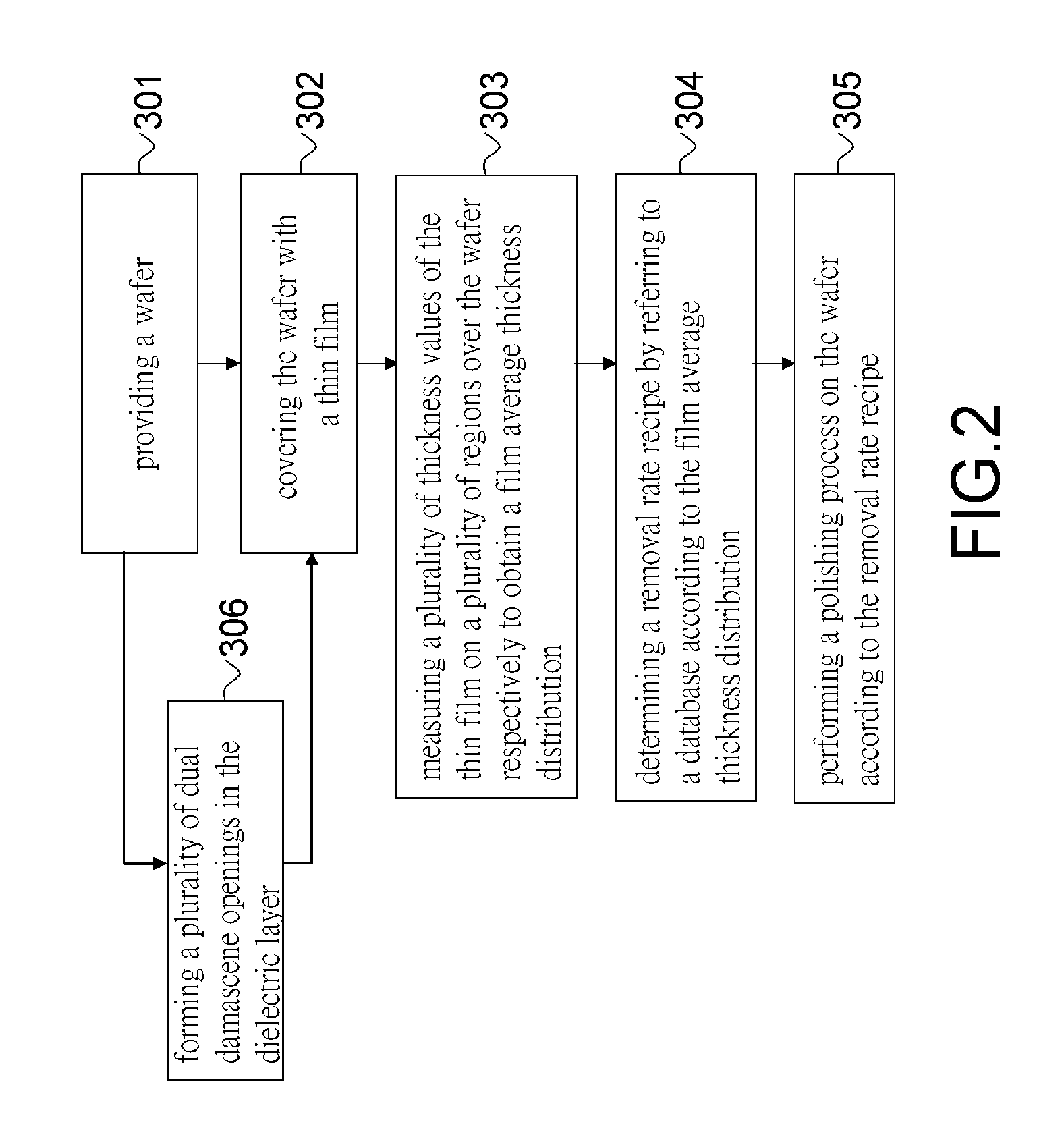
[0033]FIG. 1 shows a top view of a wafer 100 and a cross-section view of the wafer 100 along line I-I′ according to a preferred embodiment of the invention. FIG. 2 is a flow chart illustrating a method for controlling a polishing process according to one embodiment of the present invention.

[0034] As shown in FIG. 1 and FIG. 2, in the step S301, a wafer 100 is provided. The wafer 100 can be, for example but not limited to, a 12 inch wafer. In the step S302, a thin film 102 is form to cover the wafer 100. The thin film 102 can be, for example but not limited to, made of copper. The method for forming the thin film 102 can be, for example but not limited to, a electroplating process or a chemical vapor deposition process.

[0035] In the step S303, several thickness values of the thin film 102 are obtained by measuring the thickness of the thin film 102 on several regions of the wafer 100 so as to obtain a film average thickness distribution 104. The “film average thickness distribution...


PUM

PropertyMeasurementUnit
thicknessaaaaaaaaaa
thickness distributionaaaaaaaaaa

Abstract

The invention is directed to a method for controlling a polishing process. The method comprises steps of providing a first wafer, wherein a thin film is located over the first wafer. A film average thickness distribution is obtained by measuring a plurality of thickness values of the thin film on a plurality regions over the wafer respectively. A removal rate recipe is determined according to the film average thickness distribution. A polishing process is performed according to the removal rate recipe.

Description

BACKGROUND OF THE INVENTION [0001] 1. Field of Invention [0002] The present invention relates to a method for controlling a semiconductor manufacturing process. More particularly, the present invention relates to a method for controlling a polishing process. [0003] 2. Description of Related Art [0004] The chemical mechanical polishing process is widely applied on the method for forming a structure, such as dual damascene, a metal plug and a top electrode of the trench capacitor, and on the planarization of the dielectric layer and becomes an indispensable process for manufacturing the integrated circuit. [0005] In the chemical mechanical polishing process, the major process parameters include the pressure value applied on the polishing head, the composition of the slurry and the polishing particles, the material of the polishing pad, the relative linear rate between the wafer and the polishing pad and the temperature. However, the polishing result of the chemical mechanical polishin...

Claims


Application Information

Patent Timeline
Patent Type & Authority Applications(United States)
IPC IPC(8): C03C15/00H01L21/461H01L21/302B44C1/22
CPCH01L21/3212H01L21/32125H01L21/7684H01L22/26H01L2924/0002H01L2924/00
Inventor TENG, CHING-WENLIN, CHIN-KUNNEO, BOON TIONG
Owner UNITED MICROELECTRONICS CORP
Why Eureka
Try Eureka