Eureka AIR delivers breakthrough ideas for toughest innovation challenges, trusted by R&D personnel around the world.

High impedance electromagnetic surface and method

Inactive Publication Date: 2007-06-21
MOTOROLA SOLUTIONS INC
View PDF9 Cites 47 Cited by
  • Summary
  • Abstract
  • Description
  • Claims
  • Application Information

AI Technical Summary

Problems solved by technology

The ground plane, however, can degrade the performance of the antenna unless the antenna is placed a quarter wavelength away from the ground plane, which results in constructive interference between the radiated and reflected fields.
In addition, propagating surface waves lead to the undesirable characteristics of power loss, variations in radiation patterns due to ground plane edge effects, and, when antennas share a common ground plane, coupling that can result in unwanted radiation pattern nulls.
There are problems, however, associated with such prior art high impedance surfaces.
This, of course, presents problems for platforms that rely upon lower frequency bands, such as many commercial and military wireless applications in the commercial cellular (about 800-2500 MHz), ultra high frequency (UHF) (about 300-1000 MHz), and very high frequency (VHF) (less than 300 MHz) bands.
Many existing high impedance surfaces are also relatively thick, which is undesirable for many applications for which thickness and weight must be minimized.

Method used


Image

  • High impedance electromagnetic surface and method
  • High impedance electromagnetic surface and method
  • High impedance electromagnetic surface and method

Examples


Embodiment Construction

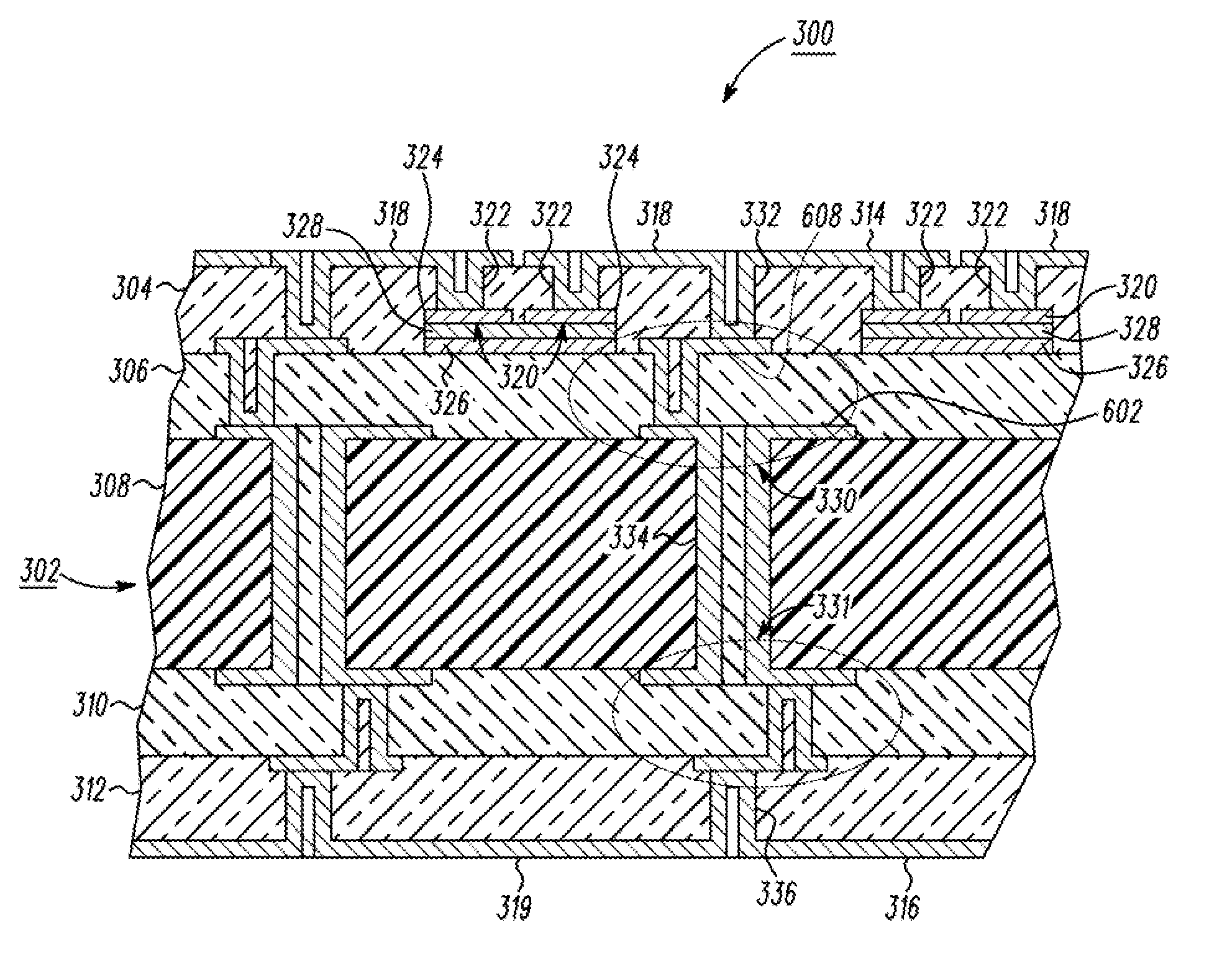
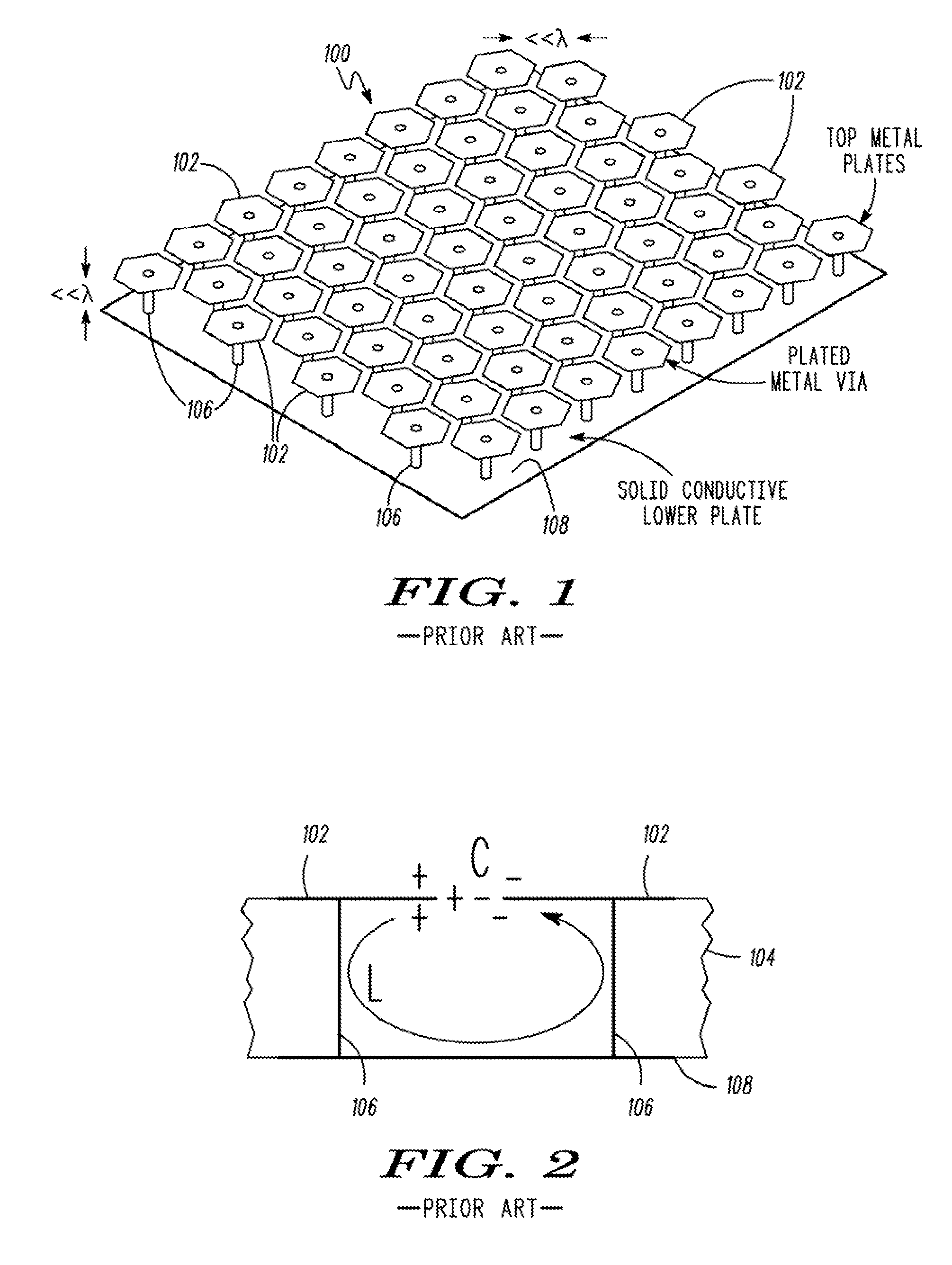
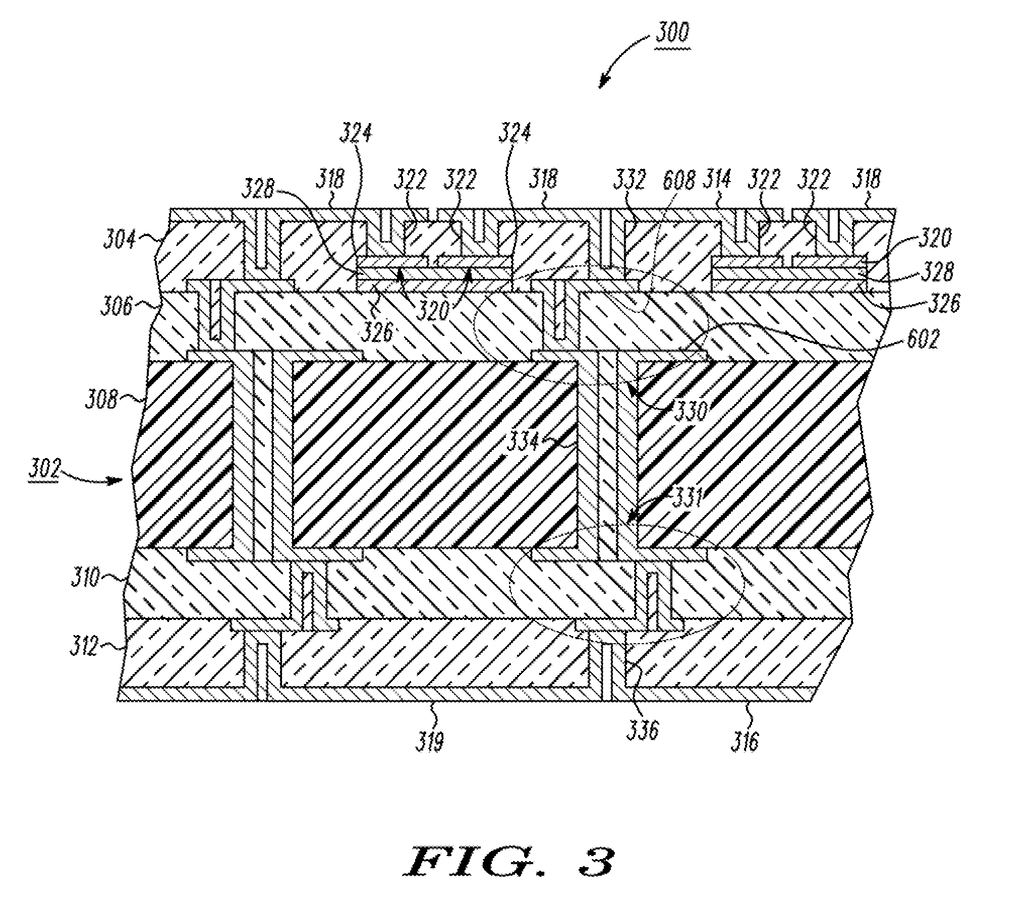
[0018] Generally, the invention is directed to a high impedance surface with embedded elements such as capacitors and inductors. Here, a high impedance surface refers to any structure that reduces surface wave propagation.

[0019] The high impedance surface is configured, in one aspect of the invention, to comprise a printed circuit board with a first surface and a second surface. A continuous electrically conductive plate is disposed on the second surface of the printed circuit board to be used as a ground plane. A plurality of electrically conductive plates is disposed on the first surface of the printed circuit board and is electrically coupled to the ground plane by conductive vias extending through the printed circuit board.

[0020] The high impedance surface also has a plurality of elements where each element is at least one of (1) at least one multi-layer inductor electrically coupled between at least two of the electrically conductive plates and embedded within the printed cir...


PUM


Abstract

A high impedance surface (300) has a printed circuit board (302) with a first surface (314) and a second surface (316), and a continuous electrically conductive plate (319) disposed on the second surface (316) of the printed circuit board (302). A plurality of electrically conductive plates (318) is disposed on the first surface (314) of the printed circuit board (302), while a plurality of elements are also provided. Each element comprises at least one of (1) at least one multi-layer inductor (330, 331) electrically coupled between at least two of the electrically conductive plates (318) and embedded within the printed circuit board (302), and (2) at least one capacitor (320) electrically coupled between at least two of the electrically conductive plates (318). The capacitor (320) comprises at least one of (a) a dielectric material (328) disposed between adjacent electrically conductive plates , wherein the dielectric material (328) has a relative dielectric constant greater than 6, and (b) a mezzanine capacitor embedded within the printed circuit board (302).

Description

FIELD OF THE INVENTION [0001] This invention relates generally to high impedance electromagnetic surfaces for antennas. BACKGROUND OF THE INVENTION [0002] Known radio frequency and microwave antennas used in handheld, laptop computer, and vehicular communication systems, for example, have a ground plane either by necessity, such as the ground plane of the printed circuit board in a cellular telephone or the metal surface of the vehicle, or intentionally to direct most of the radiation to a particular hemisphere of the antenna. The ground plane, however, can degrade the performance of the antenna unless the antenna is placed a quarter wavelength away from the ground plane, which results in constructive interference between the radiated and reflected fields. In addition, propagating surface waves lead to the undesirable characteristics of power loss, variations in radiation patterns due to ground plane edge effects, and, when antennas share a common ground plane, coupling that can res...

Claims


Application Information

Patent Timeline
IPC IPC(8): H01Q15/24
CPCH05K1/116H05K1/162H05K1/165H05K3/429H05K3/4602H05K3/4688H05K2201/0187H05K2201/0715H05K2201/09509H05K2201/09609H01Q15/006
Inventor DUNN, GREGORY J.CROSWELL, ROBERT T.KUMPF, GEORGE H.SVIGELJ, JOHN A.
Owner MOTOROLA SOLUTIONS INC
Why Eureka
Eureka Blog
Learn More