Feature failure correlation

a technology of failure correlation and feature, applied in the field of feature failure correlation, can solve the problems of increasing the number of defects that occur, the operation of the microcircuit to fail, and the difficulty of correct manufacturing, so as to reduce the the largest impact on the manufacturing yield of the integrated circui

Active Publication Date: 2007-06-21
SIEMENS PROD LIFECYCLE MANAGEMENT SOFTWARE INC
View PDF16 Cites 45 Cited by
  • Summary
  • Abstract
  • Description
  • Claims
  • Application Information

AI Technical Summary

Benefits of technology

[0011] Accordingly, various examples of the invention can be used to identify those features in an integrated circuit design will have the largest impact on the manufacturing yield of the integrated circuit. Based u...

Problems solved by technology

As microcircuit devices become more complex and their circuit elements smaller, they also become more difficult to correctly manufacture.
For example, a conventional microcircuit device may have millions of different connections, and even a single broken or shorted connection may cause the operation of the microcircuit to fail.
The complexity of the design and manufacturing process for modern integrated circuits constructed ...

Method used


Image

  • Feature failure correlation
  • Feature failure correlation
  • Feature failure correlation

Examples


Embodiment Construction

Overview

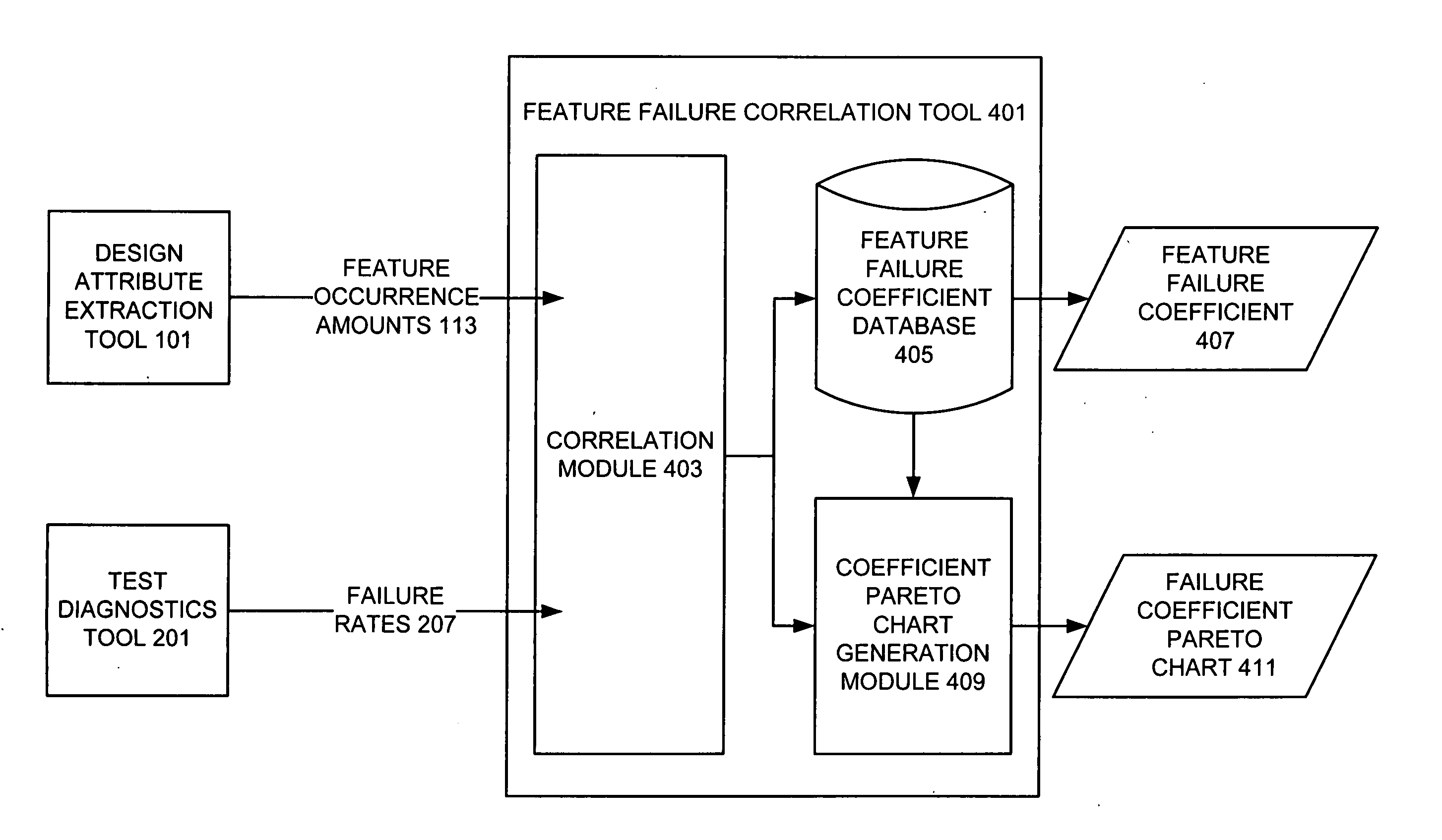
[0021] Different embodiments of the invention provide techniques for determining the likelihood that a designated feature in an integrated circuit design will cause a defect during the manufacturing process. Some implementations of the invention may also identify one or more additional, previously unrecognized design features that are likely to cause a defect. Thus, using various examples of the invention, a designer can identify those features in an integrated circuit design will have the largest impact on the manufacturing yield of the integrated circuit. A designer can then use this information to modify an integrated circuit design to reduce or avoid the use of design features that will be more likely to reduce the yield of integrated circuits manufactured from the design.

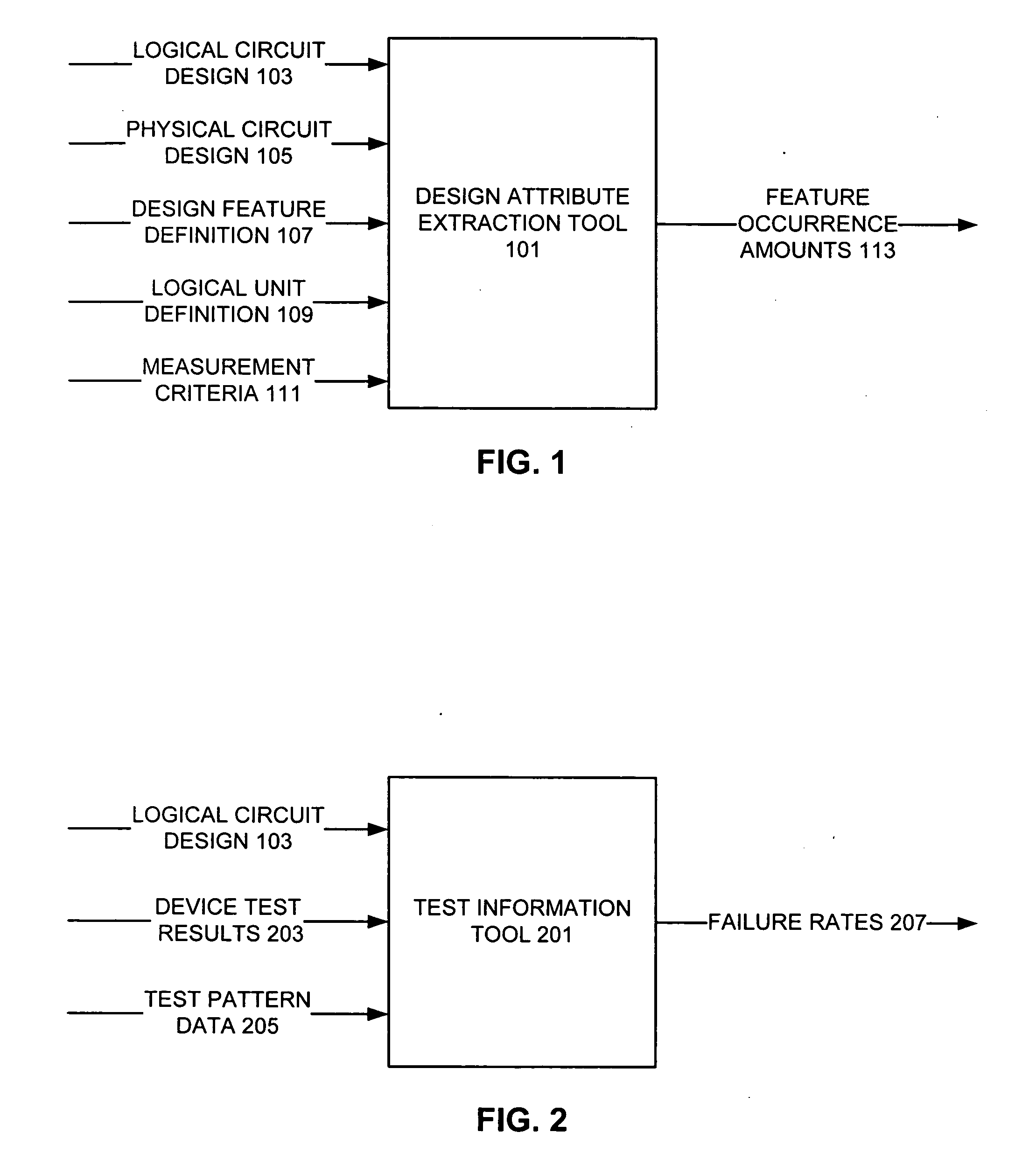
[0022] According to various embodiments of the invention, a designer initially will specify a design feature for analysis by a feature failure correlation tool. Using, for example, information provid...


PUM


Abstract

Techniques are disclosed for determining the likelihood that a known feature in an integrated circuit design will cause a defect during the manufacturing process. According to some of these techniques, various logical units that incorporate an identified design feature are identified, and the amount that the design feature occurs in each of a plurality of these logical units is determined. The failure rate of integrated circuit portions corresponding to at least these logical units are then obtained. A feature failure coefficient indicating the likelihood that the feature will cause a defect then is determined by correlating the failure rates with the amount of occurrences of the feature.

Description

RELATED APPLICATIONS [0001] This application claims priority to and is a continuation-in-part of provisional U.S. Application No. 60 / 615,329, filed on Oct. 1, 2004, entitled “Meeting Nanometer DPM Requirements Through DFT,” naming David Abercrombie et al. as inventors, which application is incorporated entirely herein by reference.FIELD OF THE INVENTION [0002] The present invention relates to various techniques and tools to assist in the design of integrated circuits. Various aspects of the present invention are particularly applicable to the use of test data to determine the physical features of an integrated circuit that are most likely to cause the integrated circuit to fail. BACKGROUND OF THE INVENTION [0003] Microcircuit devices, commonly referred to as “integrated circuits,” are used in a variety of products, from automobiles to microwaves to personal computers. Designing and fabricating integrated circuits involves many steps; which has become known as a ‘design flow,’ the pa...

Claims


Application Information

Patent Timeline
IPC IPC(8): G06F17/50
CPCG06F17/5009G06F17/5045G06F17/5068G06F2217/10G06F2217/12G06F2217/70G06F2111/08G06F2117/02G06F2119/18G06F30/39G06F30/30G06F30/20Y02P90/02
Inventor ABERCROMBIE, DAVIDFERDINEND KOONEMANN, BERND KARL
Owner SIEMENS PROD LIFECYCLE MANAGEMENT SOFTWARE INC
Why Eureka
Try Eureka