Liquid crystal display device and manufacturing method for the same

a technology of liquid crystal display and manufacturing method, which is applied in static indicating devices, instruments, non-linear optics, etc., can solve the problems of reducing image contrast, difficult process for forming ruggedness on the surface of reflection electrodes, and reducing visibility, so as to improve display quality, improve display quality, and improve the effect of luminance display

Inactive Publication Date: 2007-06-28
SHARP KK
View PDF23 Cites 0 Cited by
  • Summary
  • Abstract
  • Description
  • Claims
  • Application Information

AI Technical Summary

Benefits of technology

[0033] An object of the present invention is to provide a liquid crystal display device of those with high resolution, excellent in reflection characteristics compared with a conventional one, and a manufacturing method for the same.
[0034] Another object of the present invention is to provide a transflective type liquid crystal display device which can be manufactured more easily than a conventional one and is good in reflection characteristics and transmission characteristics, and a manufacturing method for the same.
[0035] Further another object of the present invention is to provide a liquid crystal display device having good display quality.

Problems solved by technology

However, the process for forming ruggedness on the surface of the reflection electrode is complicated in the above-described method.
However, when its neighborhood is dark, the visibility thereof is extremely decreased.
Therefore, such a reflection type liquid crystal display device poses a problem that contrast of an image is lowered and sufficient visibility is not obtained compared with the reflection type liquid crystal display device without any front light unit.
Therefore, the utilization efficiency of light is bad, involving a problem that satisfactory visibility cannot be obtained unless a backlight having large luminance is used.
However, in the case of a large-sized liquid crystal display device, it is extremely difficult to form an Al thin film having a uniform thickness over the entire surface of a panel.
Accordingly, there arises a problem that many processes are required, involving an increase in product costs.
Therefore, it is difficult to obtain a satisfactory liquid crystal display device in reflection characteristics as well as in transmission characteristics.
When the color purity of the CF layers is adjusted so that a bright display can be obtained when displaying in the reflection mode, the color purity in the transmission mode is deteriorated, resulting in a display in light colors.
Conversely, when the color purity of the CF layers is adjusted so that satisfactory color rang can be obtained when displaying in the transmission mode, reflected light is lowered when displaying in the reflection mode, resulting in an extremely dark display.
However, this structure involves a problem that display quality is greatly changed when the reflection mode and the transmission mode are switched with each other.
Moreover, in the reflection mode, a full-color display cannot be provided, involving a problem that a transmittable information quantity for users via the display screen is reduced and good display quality cannot be obtained.
Therefore, it is difficult to improve both of the reflection characteristics and the transmission characteristics, raising a problem that utilization efficiency of light is degraded.
However, an increase in a drive circuit leads to an increase in the manufacturing costs, and therefore the liquid crystal display device provided with the picture elements of six colors may not be practical.
In addition, the above structure is not applicable to the transflective type liquid crystal display device.
However, this transflective type liquid crystal display device still has such problems as will be described below. FIG. 6 shows a schematic sectional structure of three picture elements of the liquid crystal display device taken along the line II-II of FIG. 4.
Therefore, there arises a problem that color purity is made to be different between the transmission mode display and the reflection mode display, thereby degrading display quality.
For this reason, there arises a problem that when the alignment deviation is generated, color purity is made to be different between the transmission mode display and the reflection mode display, thereby degrading the display quality.

Method used


Image

  • Liquid crystal display device and manufacturing method for the same
  • Liquid crystal display device and manufacturing method for the same
  • Liquid crystal display device and manufacturing method for the same

Examples


first embodiment

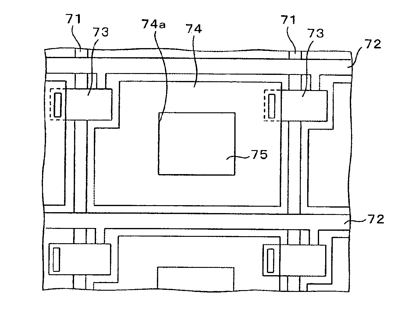
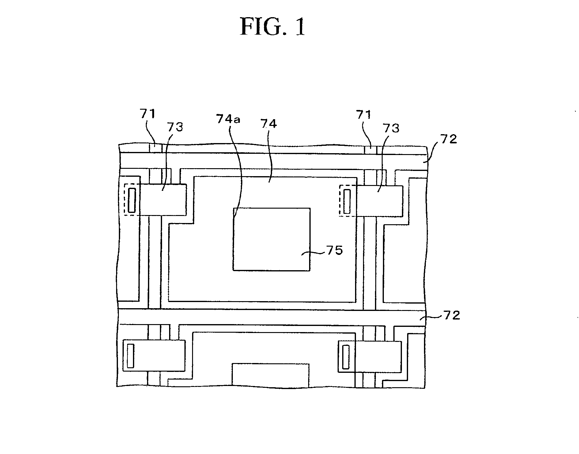
[0080]FIG. 7 is a plan view showing a liquid crystal display device of a first embodiment of the present invention, and FIG. 8 is a schematic sectional view taken along the line III-III of FIG. 7. Note that this embodiment shows an example in which the present invention is applied to a transflective type liquid crystal display device using a VA (vertically aligned) type liquid crystal.

[0081] As shown in FIG. 8, the liquid crystal display device of this embodiment is constituted including a TFT substrate 10 and a counter substrate 30, and a vertically aligned nematic liquid crystal 40. The TFT substrate 10 and the counter substrate 30 face each other, and the vertically aligned nematic liquid crystal 40 is enclosed between these substrates. Polarizing plates (linear polarizing plate or circular polarizing plate having the linear polarized light +fÉ / 4 phase difference combined) 38 and 39 are arranged under the TFT substrate 10 and on the counter substrate 30, respectively. In additio...

second embodiment

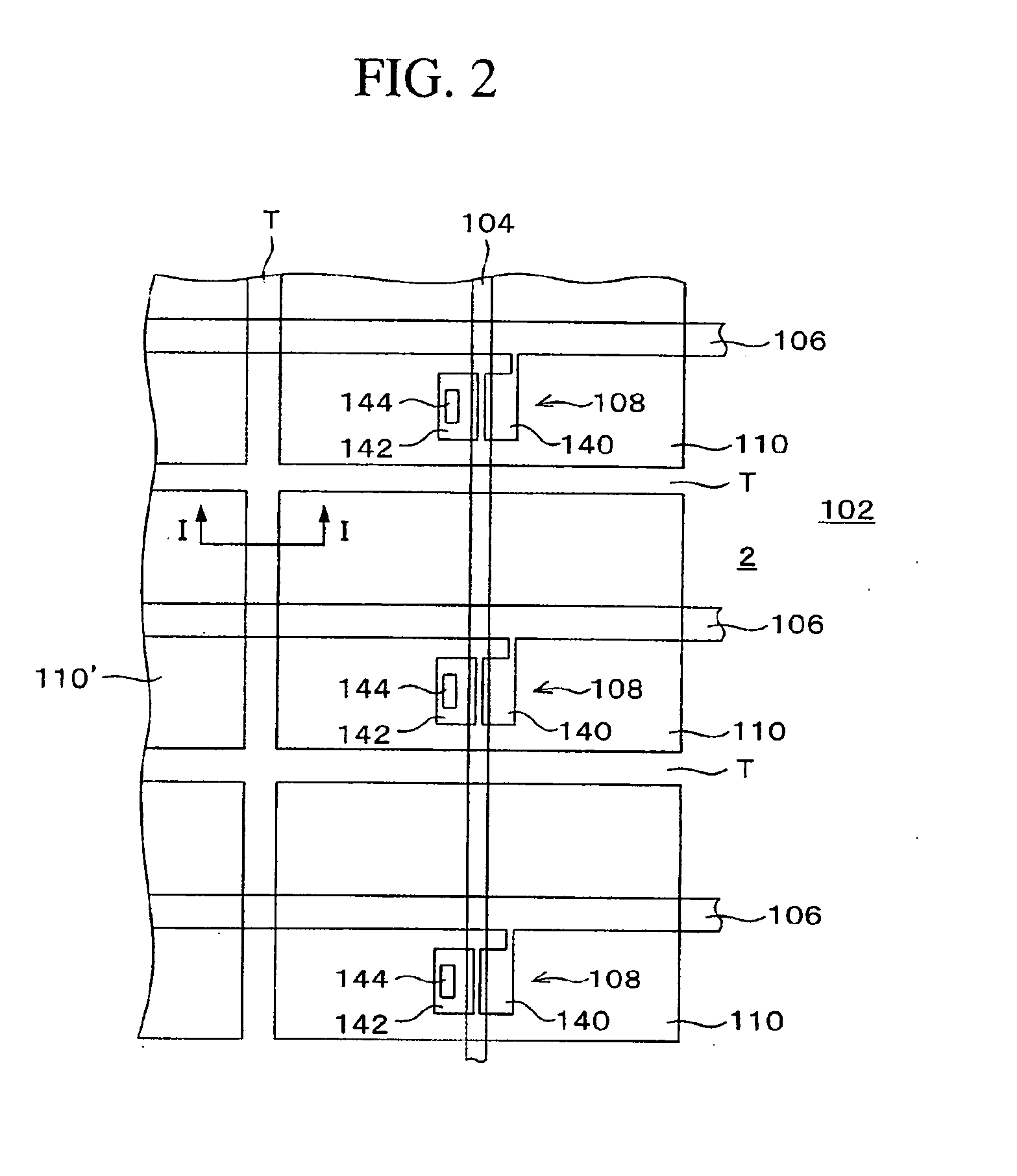
[0115]FIG. 13A is a plan view showing a transflective type liquid crystal display device of a second embodiment of the present invention. This embodiment is different from the first embodiment in that the reflection electrode is provided with slits. The other structure is basically the same as that of the first embodiment, and therefore overlapping explanation will be omitted.

[0116] In this embodiment, as shown in FIG. 13A, a plurality of slits 52 are provided on a reflection electrode 51 and a resist film disposed thereunder, in parallel to the gate bus line 12a. That is, by these slits 52, the resist film is divided into a plurality of regions in one picture element.

[0117] As described before, a rugged pattern formed on the resist film is determined depending on the size of the resist film. Like this embodiment, by providing the slits 52 on the reflection electrode 51 and the resist film thereunder, a desired rugged pattern can be formed on the reflection electrode 51 even when ...

third embodiment

[0121]FIG. 16A is a plan view showing a transflective type liquid crystal display device of a third embodiment of the present invention. Note that this embodiment is different from the first embodiment in that the reflection electrode is not provided with a rugged surface, and the reflection electrode is provided with slits. The other structure is basically the same as that of the first embodiment, and therefore overlapping explanation will be omitted.

[0122] In this embodiment, as shown in FIG. 16A, a reflection electrode 61 is provided with slits 62, and slit 62 portions serve as transmission regions. Slits 63 and 64 in the shapes as shown in FIGS. 16B and 16C, respectively, may also be provided. However, the shapes of the slits are preferably common to each picture element. Moreover, any short side of the regions divided by the slits is preferably 5 μm or more.

[0123] In this embodiment, the reflection electrode 61 is formed so as to overlap the gate bus line 12a, the data bus li...


PUM

PropertyMeasurementUnit
lengthaaaaaaaaaa
temperatureaaaaaaaaaa

Abstract

On a glass substrate, gate bus lines, data bus lines, and TFTs are formed. Then, on the substrate, an insulating film, covering the gate bus lines, data bus lines and TFTs, is formed, and a positive type photoresist film is further formed thereon. Next, through exposure and development processes, the resist film is divided for each picture element and subjected to ultraviolet ray irradiation to harden only a surface layer thereof. Then, the resist film is subjected to heat treatment to form thereon wrinkle-form surface ruggedness of a uniform pattern, which is determined depending on the size of the resist film. Subsequently, reflection electrodes are formed on the resist film. The reflection electrodes are formed to overlap the gate bus line, data bus line and TFTs, and the regions between the adjacent reflection electrodes serve as light transmission regions.

Description

[0001] This is a divisional of application Ser. No. 10 / 701,305, filed Nov. 4, 2003. CROSS-REFERENCE TO RELATED APPLICATIONS [0002] This application is based upon and claims priority of Japanese Patent Applications No. 2002-347077, filed on Nov. 29, 2002, and No. 2002-323073, filed on Nov. 6, 2002, the contents being incorporated herein by reference.BACKGROUND OF THE INVENTION [0003] 1. Field of the Invention [0004] The present invention relates to a liquid crystal display device having a reflection electrode and a manufacturing method for the same and, more particularly, to a liquid crystal display device applicable to a transflective type liquid crystal display device which can be used as a reflection type liquid crystal display device in the environment of a bright ambient, and can be used as a transmission type liquid crystal display device by switching on a backlight in the environment of a dark ambient, and a manufacturing method for the same. [0005] 2. Description of the Prior...

Claims


Application Information

Patent Timeline
Patent Type & Authority Applications(United States)
IPC IPC(8): G02F1/1335G09G3/36
CPCG02F1/133371G02F1/133514G02F1/133553G02F1/133555G02F1/133707G02F1/133753G02F1/1393G02F2203/09
Inventor OHMURO, KATSUFUMISUGIURA, NORIOTASHIRO, KUNIHIROKOIKE, YOSHIO
Owner SHARP KK
Why Eureka
Try Eureka