Liquid crystal display device and terminal device that uses same

a liquid crystal display device and terminal technology, applied in liquid crystal compositions, instruments, chemistry apparatus and processes, etc., can solve the problems of liquid crystal molecules not being able to stand completely upright, the inversion of grayscale was relatively insignificant, and the above-mentioned conventional liquid crystal display devices

Active Publication Date: 2007-06-28
NEC LCD TECH CORP
View PDF4 Cites 26 Cited by
  • Summary
  • Abstract
  • Description
  • Claims
  • Application Information

AI Technical Summary

Benefits of technology

[0058] The present invention provides an IPS liquid crystal display device having a parallel electrode pair wherein the electrode width of the parallel electrode pair is made smaller than the thickness of the liquid crystal layer, the orientation of liquid crystal molecules between the electrodes is changed by the electric field generated by the parallel electrode pair, the orientation of liquid crystal molecules disposed above the electrodes is changed in the same direction as in the liquid crystal molecules between

Problems solved by technology

This problem of grayscale inversion was relatively insignificant in mobile telephones and other terminal devices when the display content consisted mainly of telephone numbers and other characters.
However, due to the effects of the orienting force of the orientation film that determines the initial orientation, the liquid crystal molecules cannot stand completely upright even when a high voltage is applied near the boundary of the substrate, and the liquid crystal molecules are oriented in a direction that is tilted with respect to the substrate.
However, the aforementioned conventional liquid crystal display device has such problems as the following.
Specifically, since liquid crystal m

Method used


Image

  • Liquid crystal display device and terminal device that uses same
  • Liquid crystal display device and terminal device that uses same
  • Liquid crystal display device and terminal device that uses same

Examples


first embodiment

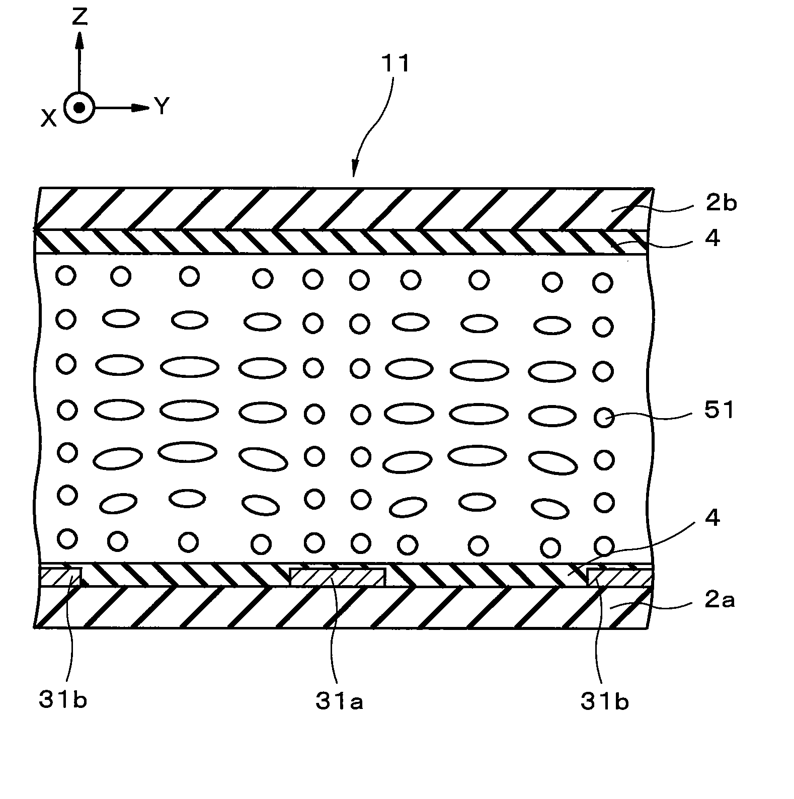
[0094] The liquid crystal display device, and the terminal device that uses the liquid crystal display device according to embodiments of the present invention, will be described in detail hereinafter with reference to the accompanying drawings. The liquid crystal display device, and the terminal device that uses the liquid crystal display device according to the present invention, will first be described. FIG. 3 is a sectional view showing a state in which a voltage is applied in the liquid crystal display device according to the present embodiment, FIG. 4 is a sectional view showing the orientation state of liquid crystal molecules when a voltage is not applied between the shared electrode and pixel electrode that are constituent elements of the present embodiment, and FIG. 5 is a perspective view showing a terminal device equipped with the liquid crystal display device according to the present embodiment.

[0095] In the liquid crystal display device 1 according to the present embod...

second embodiment

[0138] The liquid crystal display device according to the present invention will next be described. FIG. 21 is a sectional view showing a state in which a voltage is applied in the liquid crystal display device according to the present embodiment. FIG. 22 is a sectional view showing the orientation state of liquid crystal molecules when a voltage is not applied between the shared electrode and pixel electrode that are constituent elements of the present embodiment. FIG. 23 is a graph obtained by measuring the voltage-transmittance characteristics in a region that has a diameter of 100 μm and includes an area above the electrodes and between the electrodes.

[0139] As shown in FIG. 21, the liquid crystal display device 12 according to the present embodiment differs from the liquid crystal display device 1 of the first embodiment in that a pixel electrode 32a and a shared electrode 32b having a width of 1.5 μm are used instead of a pixel electrode 3a and a shared electrode 3b having a w...

third embodiment

[0146] The liquid crystal display device according to the present invention will next be described. FIG. 26 is a graph obtained by measuring the voltage-transmittance characteristics in a region that has a diameter of 100 μm and includes an area above the electrodes and between the electrodes in the liquid crystal display device according to the present embodiment.

[0147] The liquid crystal display device according to the present embodiment differs from the liquid crystal display device 12 of the second embodiment in that a pixel electrode and a shared electrode having a width of 1 μm are used instead of a pixel electrode 32a and a shared electrode 32b having a width of 1.5 μm. The gap between the pixel electrode and the shared electrode, i.e., the inter-electrode distance, is set to 1 μm in the present embodiment, whereas this distance was set to 3.8 μm in the second embodiment. The cell gap is 3.5 μm, as in the second embodiment. Specifically, the present embodiment differs from th...


PUM


Abstract

In a liquid crystal display device, a liquid crystal layer is provided between a principal substrate and an opposing substrate that are disposed so as to face each other, and a shared electrode and a pixel electrode, which is a parallel electrode pair formed in the shape of a comb, are formed on the surface of the principal substrate that faces the opposing substrate. Orientation films are also formed on the opposing surfaces of the principal substrate and the opposing substrate. The electrodes of the parallel electrode pair are formed so that the width thereof is smaller than the thickness of the liquid crystal layer. The orientation of the liquid crystal molecules between the electrodes is thereby changed by an electric field generated by the parallel electrode pair, and the orientation of liquid crystal molecules disposed above the electrodes is changed in the same direction as in the liquid crystal molecules between the electrodes in accordance with the change in orientation of the liquid crystal molecules between the electrodes. A high degree of transmittance can thereby be achieved by a simple electrode structure in an in-plane switching liquid crystal display device.

Description

BACKGROUND OF THE INVENTION [0001] 1. Field of the Invention [0002] The present invention relates to a liquid crystal display device and to a terminal device, and particularly relates to an in-plane switching (IPS) liquid crystal display device wherein high transmittance can be obtained by a simple electrode structure, and to a terminal device that utilizes the liquid crystal display device. [0003] 2. Description of the Related Art [0004] Because of their thin profile, light weight, small size, low energy consumption, and other advantages, display devices that use liquid crystals have been widely deployed and used in a range of devices that includes monitors, televisions (TV), and other large terminal devices; notebook-type personal computers, cash dispensers, vending machines, and other mid-sized terminal devices; and personal TVs, PDAs (Personal Digital Assistance), mobile telephones, mobile gaming devices, and other small terminal devices. In the liquid crystal panel that is the ...

Claims


Application Information

Patent Timeline
IPC IPC(8): G02F1/1343
CPCG02F1/134363G02F2201/124
Inventor UEHARA, SHIN-ICHINIIOKA, SHINYA
Owner NEC LCD TECH CORP
Why Eureka
Try Eureka