Semiconductor device and method for fabricating the same

a technology of semiconductors and semiconductors, applied in the direction of semiconductor devices, electrical equipment, transistors, etc., can solve the problems of deteriorating transistor performance and increasing resistance, and achieve the effects of reducing interface resistance, excellent ni silicide layer, and high speed

Inactive Publication Date: 2007-07-12
PANASONIC CORP
View PDF1 Cites 4 Cited by
  • Summary
  • Abstract
  • Description
  • Claims
  • Application Information

AI Technical Summary

Benefits of technology

[0009] It is therefore an object of the present invention to form an excellent Ni silicide layer by achieving both stable formation of a NiSi layer, which is a low-resistance layer, and reduction of the interface resistance generated at the interface between NiSi and silicon.
[0020] According to the present invention, a silicide layer containing a metal silicide having an enthalpy of formation (formation enthalpy) lower than that of NiSi is provided, i.e., a silicide layer having a lattice constant different from that of silicon is provided, at the interface between silicide and silicon, so that generation of NiSi2 forming an inverted-pyramidal silicide-silicon interface caused by lattice-constant matching with silicon is suppressed. Accordingly, the NiSi layer serving as a low-resistance layer is stabilized. In addition, the provision of a silicide layer including a metal silicide having a formation enthalpy lower than that of NiSi at the interface between silicide and silicon reduces the Schottky barrier height between silicide and silicon that is proportional to the formation enthalpy. Accordingly, the interface resistance between silicide and silicon that is proportional to the exponential function of the Schottky barrier height is reduced. In this manner, both stable formation of a NiSi layer as a low-resistance layer and reduction of the interface resistance at the interface between NiSi and silicon are achieved, so that an excellent Ni silicide layer is formed. Accordingly, a semiconductor device capable of being miniaturized and operating at high speed is implemented.
[0021] As described above, the present invention relates to semiconductor devices and methods for fabricating the same. In applications to semiconductor integrated circuit devices including silicide layers, for example, miniaturization and increase of the operation speed are achieved, and thus the present invention is very useful.

Problems solved by technology

However, it is reported that in the case of forming an alloyed silicide with the foregoing conventional techniques, coexistence of different elements in a silicide layer causes alloy scattering, resulting in increase of resistance (see, for example, non-patent literature 6: F. M. d'Heurle et al., “Resistivity of the solid solutions (Co—Ni)Si2”, J. Appl. Phys. 59, 1986, pp.
The interface resistance generated at the interface between NiSi and silicon serves as parasitic resistance that effectively increases the resistances of a silicide layer and a source / drain doped layer located under the silicide layer, resulting in causing deterioration of transistor performance.

Method used


Image

  • Semiconductor device and method for fabricating the same
  • Semiconductor device and method for fabricating the same
  • Semiconductor device and method for fabricating the same

Examples


embodiment 1

[0028] Hereinafter, a semiconductor device according to a first embodiment of the present invention, specifically a semiconductor device including a MOS transistor, and a method for fabricating the device will be described with reference to the drawings.

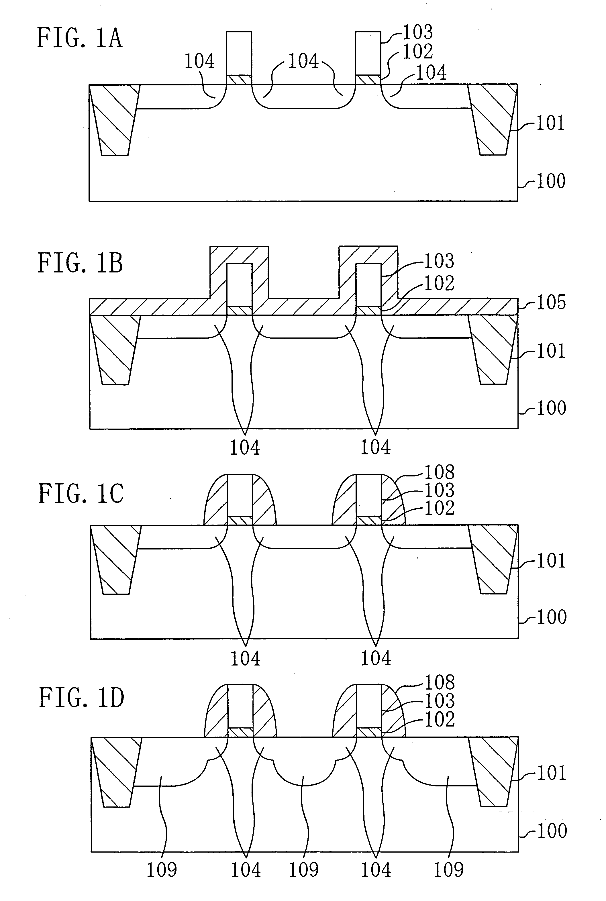
[0029]FIGS. 1A through 1D and FIGS. 2A through 2D are cross-sectional views showing process steps of a method for fabricating a semiconductor device of this embodiment.

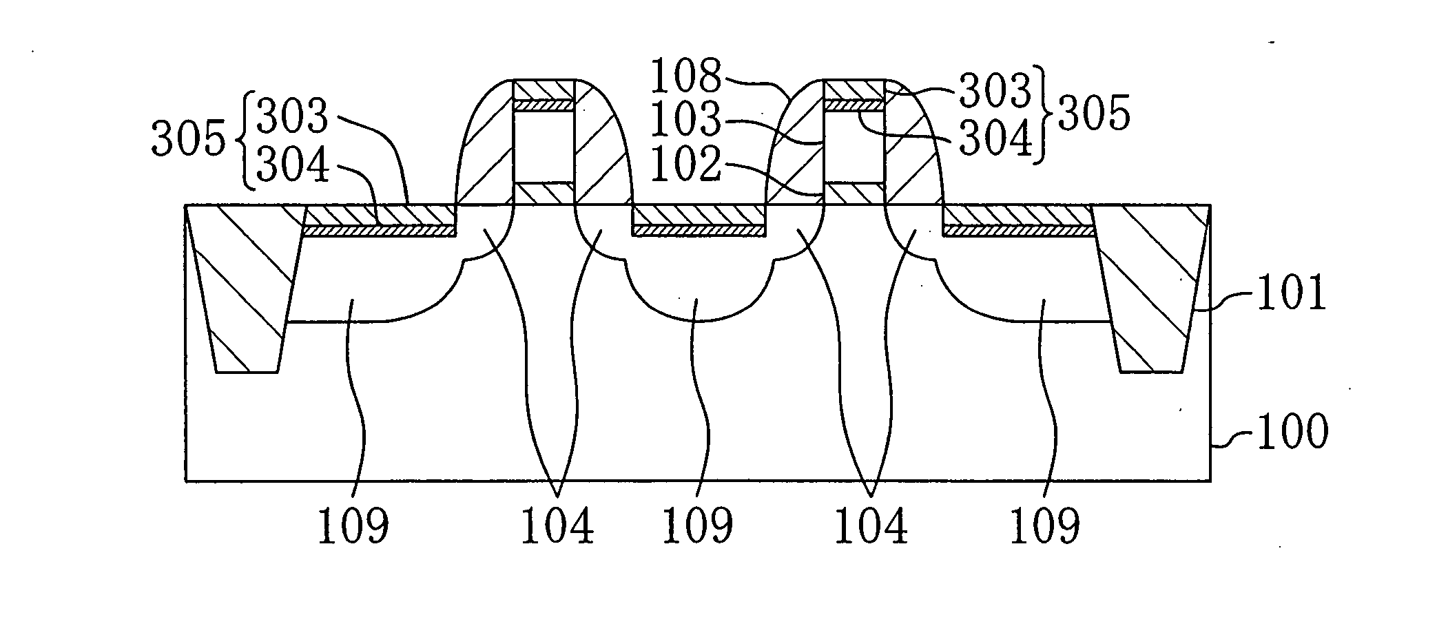
[0030] First, as shown in FIG. 1A, a shallow trench isolation 101 is formed in an upper portion of a silicon substrate 100 so as to define transistor regions. Thereafter, a gate insulating film 102 made of a silicon oxide film and having a thickness of about 2 nm is formed on the transistor regions, and then a polysilicon film having a thickness of about 140 nm is formed over the entire surface of the silicon substrate 100. Subsequently, the polysilicon film is selectively etched, thereby forming gate electrodes 103. Then, ion implantation is performed with the gate ...

embodiment 2

[0047] Hereinafter, a semiconductor device according to a second embodiment of the present invention, specifically a semiconductor device including a MOS transistor, and a method for fabricating the device will be described with reference to the drawings.

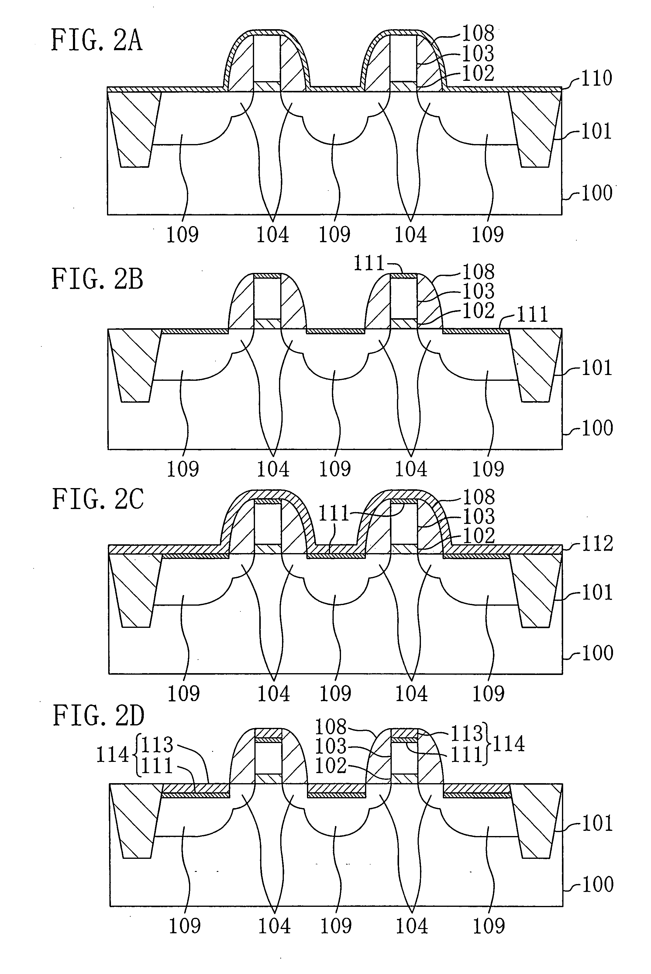
[0048]FIGS. 4A through 4C are cross-sectional views showing process steps of a method for fabricating a semiconductor device of this embodiment.

[0049] In this embodiment, first, process steps similar to those of the method for fabricating a semiconductor device of the first embodiment shown in FIGS. 1A through 1D are performed.

[0050] After the process step shown in FIG. 1D, in a silicon substrate 100 in which components to a heavily-doped layer 109 are formed, a metal capable of forming a metal silicide having a formation enthalpy lower than that of NiSi is introduced, e.g., Hf is introduced by ion implantation, in silicon portions forming the heavily-doped layer 109 to be source / drain regions and gate electrodes 103, thereby for...

embodiment 3

[0061] Hereinafter, a semiconductor device according to a third embodiment of the present invention, specifically a semiconductor device including a MOS transistor, and a method for fabricating the device will be described with reference to the drawings.

[0062]FIGS. 6A through 6C are cross-sectional views showing process steps of a method for fabricating a semiconductor device of this embodiment.

[0063] In this embodiment, first, process steps similar to those of the method for fabricating a semiconductor device of the first embodiment shown in FIGS. 1A through 1D are performed.

[0064] After the process step shown in FIG. 1D, in a silicon substrate 100 in which components to a heavily-doped layer 109 are formed, a Ni silicide film 501 is formed only on the heavily-doped layer 109 to be source / drain regions and gate electrodes 103 as in the second embodiment, as shown in FIG. 6A.

[0065] Then, as shown in FIG. 6B, a metal, such as Hf, capable of forming a metal silicide having a forma...


PUM


Abstract

A semiconductor device includes: a gate electrode formed on a silicon substrate; source / drain regions formed at both sides of the gate electrode in the silicon substrate; and a silicide layer formed on the source / drain regions. The silicide layer includes a first silicide layer mainly made of a metal silicide having a formation enthalpy lower than that of NiSi and a second silicide layer formed on the first silicide and made of Ni silicide.

Description

BACKGROUND OF THE INVENTION [0001] (1) Field of the Invention [0002] The present invention relates to semiconductor devices and methods for fabricating the same, and particularly relates to a structure of a silicide layer and a method for forming the silicide layer. [0003] (2) Description of the Related Art [0004] In general metal oxide semiconductor (MOS) transistors, reduction of parasitic resistance such as contact resistance and wiring resistance is important in increasing operation speed. The reduction of parasitic resistance in such transistors is generally achieved by siliciding upper portions of source / drain regions and upper portions of gate electrodes. [0005] To increase the integration degree of a large-scale semiconductor integrated (LSI) circuit device, reduction of the vertical size as well as the horizontal size is needed. As a technique for reducing the vertical size, the junction depth of a doped layer to be source / drain regions needs to be reduced. However, if the ...

Claims


Application Information

Patent Timeline
Patent Type & Authority Applications(United States)
IPC IPC(8): H01L29/76H01L21/4763
CPCH01L21/26506H01L21/28518H01L21/823418H01L29/7833H01L21/823443H01L29/665H01L29/6659H01L21/823425
Inventor OKUNO, YASUTOSHIMATSUMOTO, MICHIKAZU
Owner PANASONIC CORP
Why Eureka
Try Eureka