Organic electroluminescent device

a technology of electroluminescent devices and electroluminescent tubes, which is applied in the direction of discharge tube luminescent screens, natural mineral layered products, transportation and packaging, etc., can solve the problems of difficult to reduce the power consumption of flat panel displays, significant reduction of emission efficiency, etc., and achieve high current efficiency and high luminous efficiency

Active Publication Date: 2007-07-12
IDEMITSU KOSAN CO LTD
View PDF20 Cites 64 Cited by
  • Summary
  • Abstract
  • Description
  • Claims
  • Application Information

AI Technical Summary

Benefits of technology

[0014] The invention provides, a phosphorescent organic EL device, particularly emitting light in a blue region, which exhibits high current efficiency and high luminous efficiency.

Problems solved by technology

However, the above-mentioned device configuration has a disadvantage in that the emission efficiency significantly decreases accompanying an increase in luminance.
Therefore, it is difficult to reduce the power consumption of the flat panel display.

Method used


Image

  • Organic electroluminescent device
  • Organic electroluminescent device
  • Organic electroluminescent device

Examples


example 1

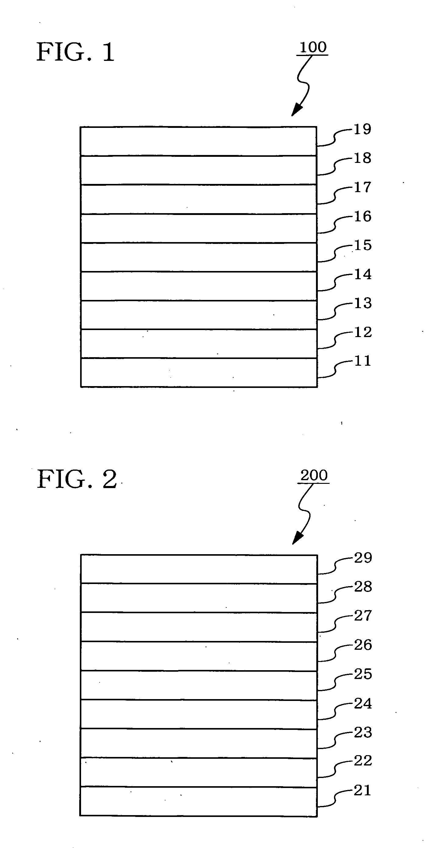
[0083] An organic EL device shown in FIG. 1 was fabricated as follows.

[0084] A glass substrate 11, measuring 25 mm×75 mm×1.1 mm thick, with an ITO transparent electrode (anode) 12 (manufactured by Geomatics Co.) was subjected to ultrasonic cleaning in isopropyl alcohol for 5 minutes and then to UV ozone cleaning for 30 minutes. The cleaned glass substrate 11 with transparent electrode lines was mounted on a substrate holder in a vacuum deposition device. First, a 100 nm thick film of N,N′-bis(N,N′-diphenyl-4-aminophenyl)-N,N-diphenyl-4,4′-diamino-1,1′-biphenyl (hereinafter referred to as TPD 232 film) 13 was formed by resistance heating deposition on the surface where the transparent electrode lines were formed, so as to cover the transparent electrode 12. This TPD 232 film 13 functioned as a hole-injecting layer (a hole-transporting layer).

[0085] After the formation of the TPD 232 film 13, a 10 nm thick hole-transporting layer (hereinafter referred to as HTM) 14 was formed by res...

example 2

[0089] An organic EL device was fabricated in the same manner as in Example 1 except that the following PC-8 was introduced by resistance heating deposition to a thickness of 30 nm as an electron-transporting layer on an emitting layer made of the host material 2: FIrpic.

example 3

[0090] An organic EL device shown in FIG. 2 was fabricated as follows.

[0091] A glass substrate 21, measuring 25 mm×75 mm×1.1 mm thick, with an ITO transparent electrode (anode) 22 (manufactured by Geomatics Co.) was subjected to ultrasonic cleaning in isopropyl alcohol for 5 minutes and then to UV ozone cleaning for 30 minutes. The cleaned glass substrate 21 with transparent electrode lines was mounted on a substrate holder in a vacuum deposition device. First, a 100 nm thick TPD 232 film 23 was formed by resistance heating deposition on the surface where the transparent electrode lines were formed, so as to cover the transparent electrode 22. The TPD 232 film 23 functioned as a hole-injecting (hole-transporting) layer.

[0092] After the formation of the TPD 232 film 23, a 10 nm thick hole-transporting layer (HTM) 24 was formed by resistance heating deposition. After the formation of the hole-transporting layer 24, a host material 1 and FIrpic were co-deposited by resistance heating...


PUM

PropertyMeasurementUnit
triplet energy gapaaaaaaaaaa
ionization potentialaaaaaaaaaa

Abstract

An organic EL device 100 including a plurality of emitting layers (15) and (17) between a cathode (18) and (19) and an anode (12), each of the emitting layers (15) and (17) made of a host material having a triplet energy gap of 2.52 eV or more and 3.7 eV or less, and a dopant having a light emitting property related to a triplet state, the dopant containing a metal complex with a heavy metal.

Description

TECHNICAL FIELD [0001] The invention relates to an organic electroluminescent device (hereinafter abbreviated as “organic EL device”). More particularly, the invention relates to a highly efficient organic EL device. BACKGROUND ART [0002] An organic EL device using an organic substance is a promising solid-state emitting type inexpensive and large full-color display device, and has been extensively developed. An EL device generally includes an emitting layer and a pair of opposing electrodes holding the emitting layer therebetween. [0003] In the EL device, electrons and holes are injected into the emitting layer from a cathode and an anode respectively upon application of an electric field between the electrodes. The electrons and the holes recombine in the emitting layer to produce an excited state, and the energy is emitted as light when the excited state returns to the ground state whereby the EL device emits light. [0004] Various configurations have been known as the configurati...

Claims


Application Information

Patent Timeline
Patent Type & Authority Applications(United States)
IPC IPC(8): H01L51/54C09K11/06H01L51/00H01L51/50H05B33/12H05B33/14
CPCC09K11/06Y10T428/24116C09K2211/1014C09K2211/1029C09K2211/1044C09K2211/186H01L51/006H01L51/0067H01L51/0071H01L51/0081H01L51/0085H01L51/0094H01L51/5016H01L51/5036H05B33/14Y10S428/917C09K2211/1007H10K85/633H10K85/654H10K85/657H10K85/324H10K85/342H10K85/40H10K50/125H10K50/11H10K2101/10H05B33/22
Inventor MATSUURA, MASAHIDEHOSOKAWA, CHISHIOIWAKUMA, TOSHIHIROYAMAMICHI, KEIKO
Owner IDEMITSU KOSAN CO LTD
Why Eureka
Try Eureka