
Built-in self test for system in package

a self-testing, integrated technology, applied in the direction of electrical testing, measurement devices, instruments, etc., can solve the problems of difficult automatic generation of suitable test patterns for the sip, inapplicability of boundary scan tests to flash memory, and difficulty in automatically creating functional patterns for interconnection, etc., to achieve the effect of low cost and easy generation

Active Publication Date: 2007-07-12
FARADAY TECH CORP
View PDF7 Cites 3 Cited by
  • Summary
  • Abstract
  • Description
  • Claims
  • Application Information

AI Technical Summary

Benefits of technology

[0008] Another aspect of the invention is to provide an easy and low-cost test circuit and configuration for testing in the SIP containing memory modules.

Problems solved by technology

But it is difficult to automatically generate suitable test patterns for the SIP integrating the ASIC and the flash memory.
However, the boundary scan test is not applicable to the flash memory, which does not have the corresponding scan chain circuit.
Additionally, it is difficult to automatically create functional patterns for the interconnection test because each creation of pattern is case-specific.

Method used


Image

  • Built-in self test for system in package
  • Built-in self test for system in package
  • Built-in self test for system in package

Examples


Embodiment Construction

[0015] Reference will now be made in detail to the present preferred embodiments of the invention, examples of which are illustrated in the accompanying drawings. Wherever possible, the same reference numbers are used in the drawings and the description to refer to the same or like parts.

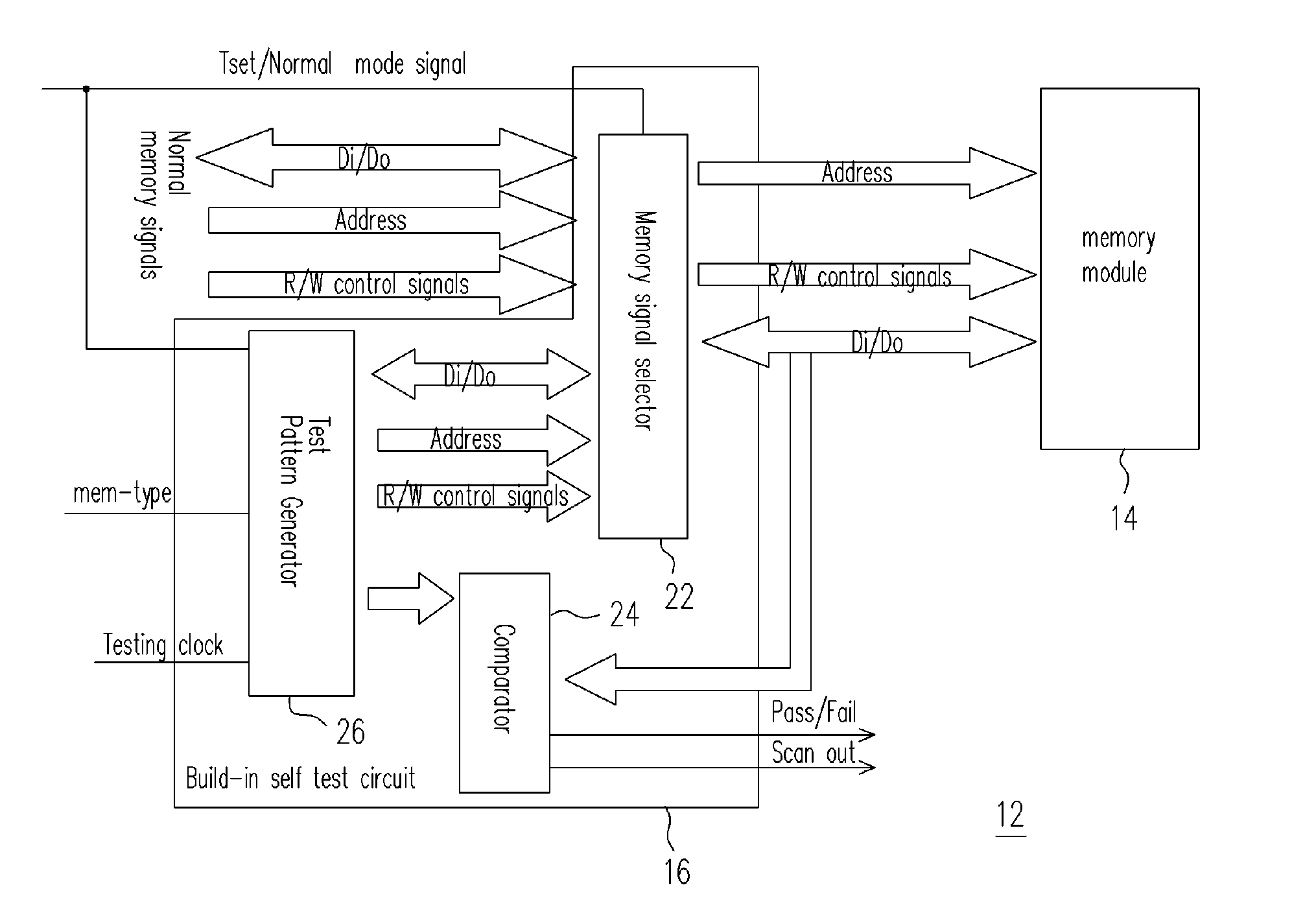
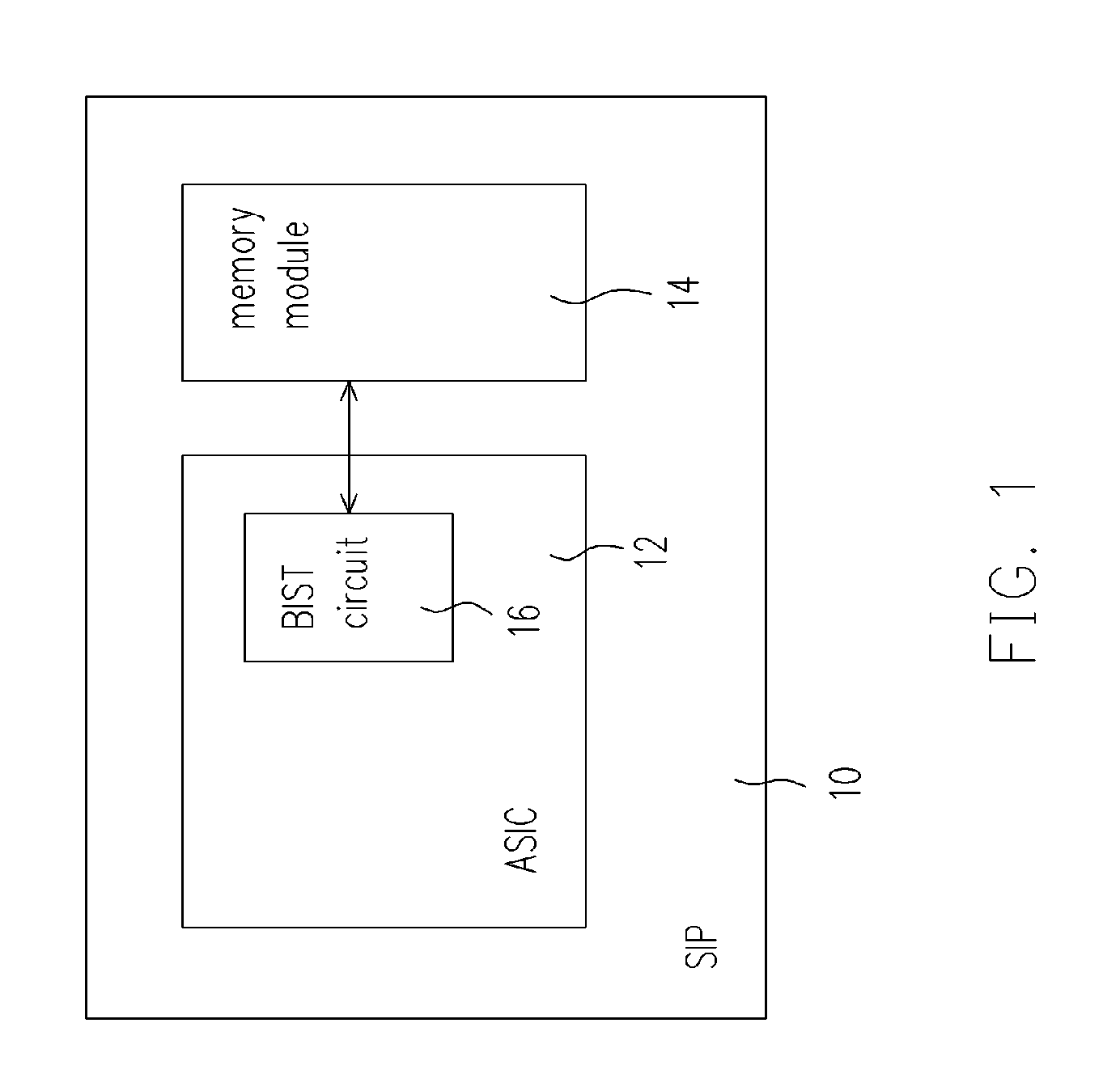
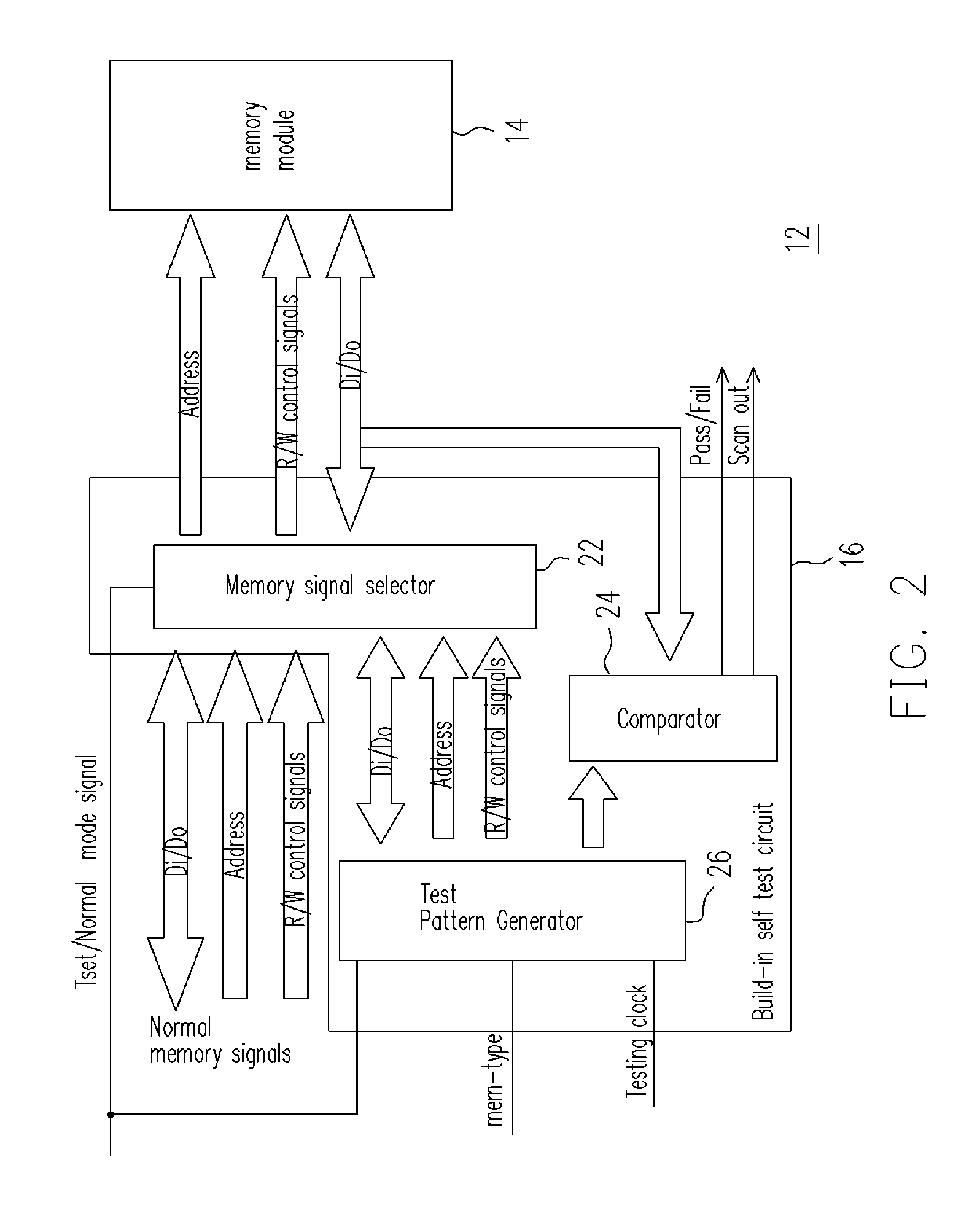
[0016] In one embodiment of the invention, a BIST (Built-In Self Test) circuit is in a memory I / O (Input / Output) interface of an ASIC of the SIP, wherein the SIP at least includes the ASIC and a memory module. The memory module does not include any scan chain for integration boundary test. The memory module is, but not limited to, a DDR (dual date rate) memory module.

[0017] Please refer to FIG. 1, which is a SIP (System in Package) diagram according to one embodiment of the invention. The SIP 10 at least includes an ASIC 12 and a memory module 14. The ASIC 12 is a SOC (System on a Chip). The memory module 14 is embedded outside of the ASIC 12. The memory module 14 does not include any scan chain w...


PUM


Abstract

A SIP (system in package) with a chip and a memory mode, capable of performing integration test on the memory module even if the memory module does not include any scan chain is provided. The chip has a built-in self-test (BIST) circuit, which generates test pattern signals to test the memory module in response to a mode signal. Under a test mode, after the memory module receives the test pattern signals, the memory module outputs responsive readout signals to the BIST circuit and the BIST circuit determines and outputs a test result and a test record in response to the readout signals. If the test fails, conditions of the faulty memory module are recognized from the test record.

Description

BACKGROUND OF THE INVENTION [0001] 1. Field of Invention [0002] The present invention relates to a configuration of SIP (System In Package), more particularly to a test configuration of the SIP for enhancing integration or interconnection scan test of memory modules in the SIP. [0003] 2. Description of Related Art [0004] Nowadays electronic devices, such as: mobile phones, PDAs (personal digital assistants) and on the likes are required to be compact and weight-light; therefore, a SIP (System In Package) technique is developed. In SIP, several chips or ICs or memory modules are integrated into one package, such as: ASIC (Application Specific Integrated Circuit) and a flash memory (memory module) packaged together to reduce the size as whole. Before being packaged, the ASIC and the flash memory are tested respectively and integrated together when they pass the test. Though the ASIC and the flash memory are good dies before being packaged, they have to be tested again after being pack...

Claims


Application Information

Patent Timeline
Patent Type & Authority Applications(United States)
IPC IPC(8): G01R31/26
CPCG01R31/31855G11C5/04G11C2029/3602G11C2029/0405G11C29/36
Inventor CHEN, WANG-JINCHANG, AVILES
Owner FARADAY TECH CORP
Learn More