Semiconductor processing apparatus with lift pin structure

a technology of lifting pin and processing apparatus, which is applied in the direction of chemistry apparatus and processes, chemical/physical/physical-chemical processes, coatings, etc., can solve the problems of inability to adjust the position, foreign matter, and heat expansion amount differences, so as to reduce the maintenance time, improve the operating rate, and reduce the contact resistance

Active Publication Date: 2007-07-12
ASM JAPAN
View PDF8 Cites 50 Cited by
  • Summary
  • Abstract
  • Description
  • Claims
  • Application Information

AI Technical Summary

Benefits of technology

[0017]Consequently, in an embodiment, the present invention relates to a mechanism supporting a semiconductor wafer inside a reaction chamber and has an objective to provide a substrate supporting mechanism which does not cause positional misalignment of a substrate lift pin with a through-hole in a susceptor.
[0018]Additionally, in an embodiment, the present invention has an objective to provide a substrate supporting mechanism in which a substrate lift pin does not cause interference with a through-hole in a susceptor.
[0019]Additionally, in an embodiment, the present invention has an objective to provide a substrate supporting mechanism which does cause malfunctions such as a substrate lift pin being stuck in or caught in a through-hole in a susceptor.
[0020]Furthermore, in an embodiment, the present invention has an objective to provide a semiconductor processing apparatus having an improved operating rate by reducing maintenance time by facilitating mounting / removing a substrate lift pin.
[0021]In an embodiment, the present invention which can achieve one or more of the above objectives provides a semiconductor processing apparatus comprising: (i) a reaction chamber; (ii) a susceptor disposed in the reaction chamber for placing a substrate thereon, said susceptor having through-holes in an axial direction of the susceptor; (iii) lift pins slidably disposed in the respective through-holes for lifting the substrate over the susceptor; and (iv) a means for reducing contact resistance between the lift pins and the respective through-holes.

Problems solved by technology

Although these conventional techniques attempt to resolve each other's problem, they have problems described below.
First, a method in which a substrate lift pin is attached on a bottom portion of a reaction chamber has a problem which an inner wall of a through-hole in a susceptor and a substrate lift pin interfere with each other.
This temperature difference causes a difference in a heat expansion amount, thereby causing position misalignment of a through-hole in a susceptor with a substrate lift pin.
Because of this positional misalignment and up-and-down movement of the susceptor, the substrate lift pin comes in contact with an inner wall of the through-hole in the susceptor, thereby causing a foreign matter.
It takes approximately 3 to 4 hours respectively for the cooling and the heating, which leads to long down time of the apparatus.
Because of this adhesion of the formed seasoning layer to the inside of the through-hole, a problem that a substrate lift pin inserted therein is stuck therein is caused.
As a result, the substrate lift pin cannot be moved inside the through-hole.

Method used


Image

  • Semiconductor processing apparatus with lift pin structure
  • Semiconductor processing apparatus with lift pin structure
  • Semiconductor processing apparatus with lift pin structure

Examples


Embodiment Construction

[0056]The present invention will be explained with respect to preferred embodiments. However, the preferred embodiments are not intended to limit the present invention.

[0057]The present invention is described by referring to figures. Additionally, “the present invention” aims to mean “an embodiment of the present invention”, but “an embodiment of the present invention” does not aim to limit the present invention thereby.

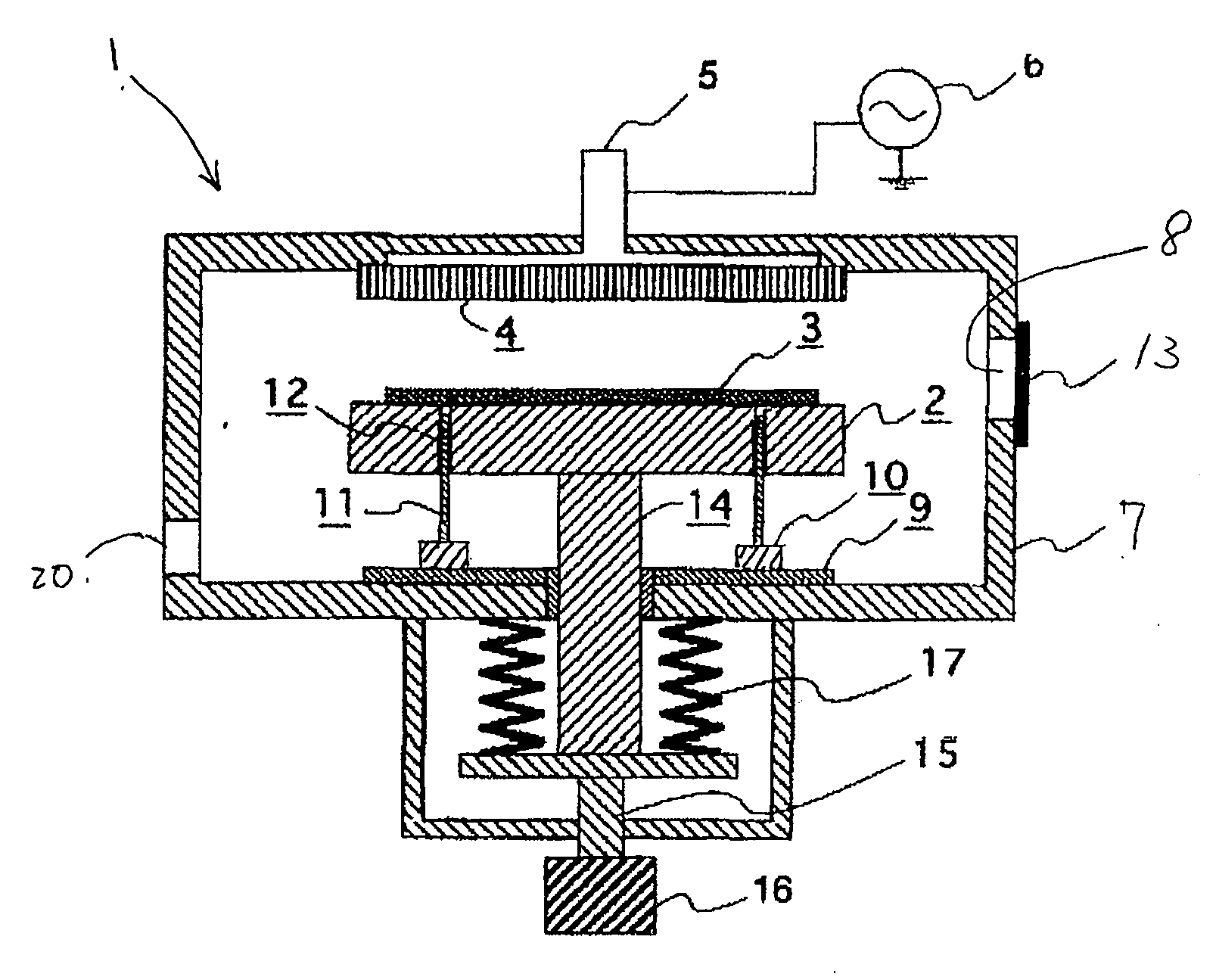
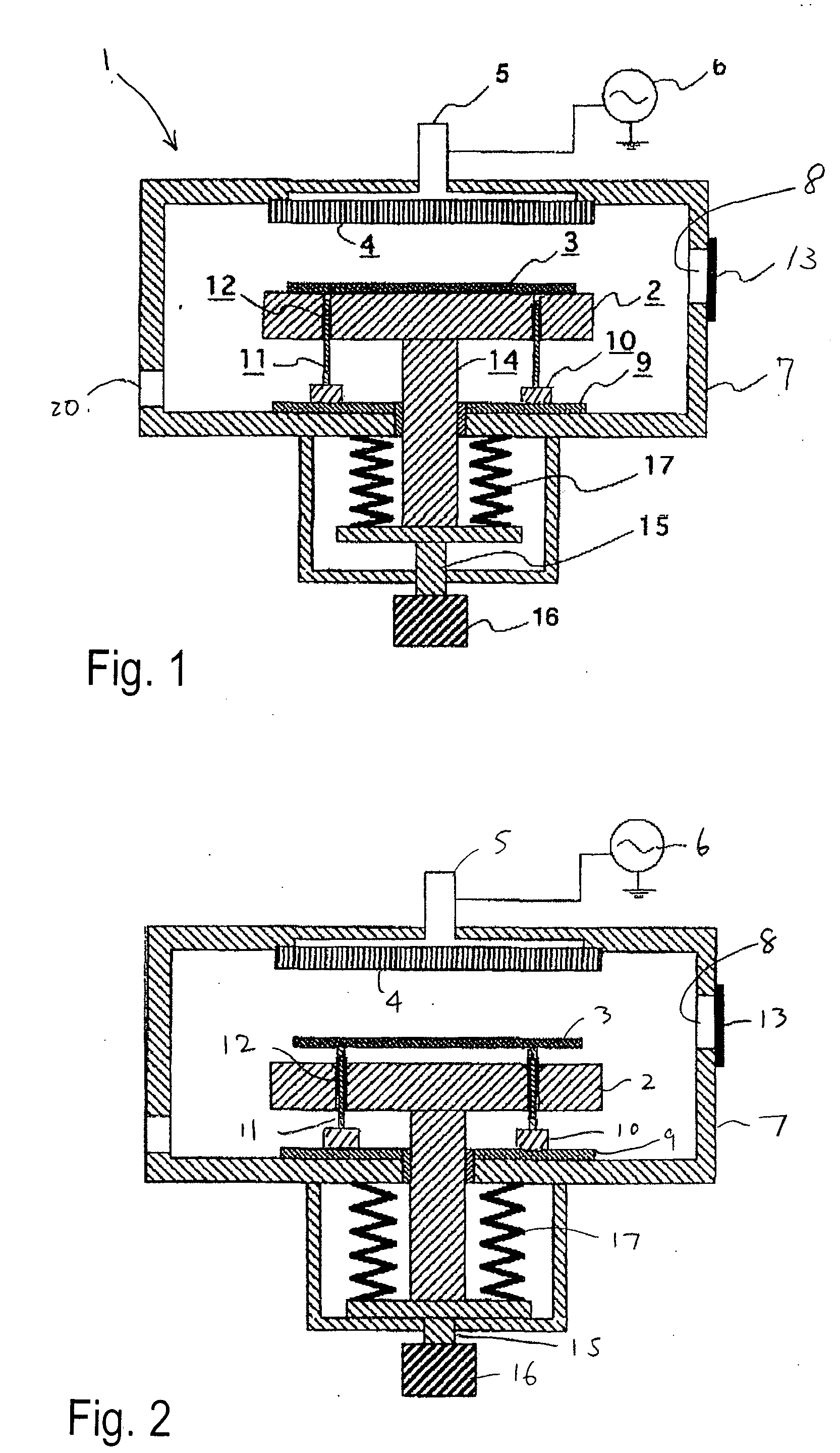
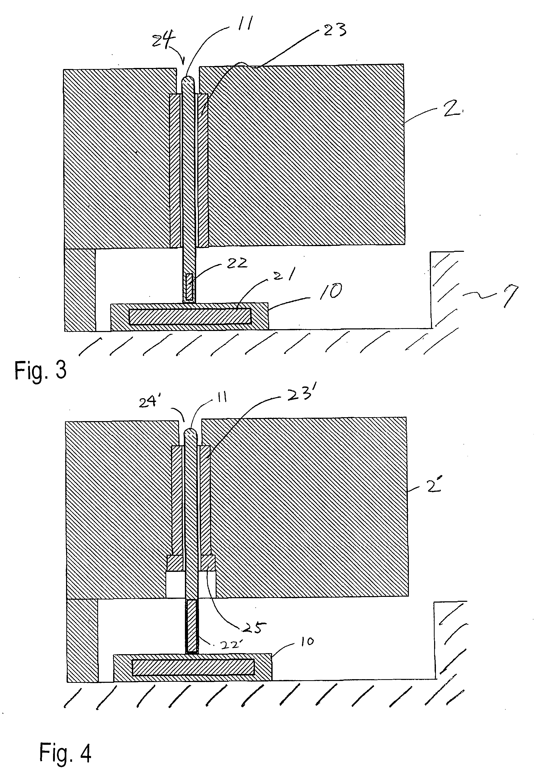
[0058]FIG. 1 is a schematic cross sectional view of a plasma CVD apparatus according to an embodiment of the present invention. The plasma CVD apparatus 1 for forming a thin film on a semiconductor wafer 3 according to the present invention comprises a reaction chamber 7, a susceptor 2 disposed inside the reaction chamber 7 for placing the semiconductor wafer 3 thereon, a showerhead 4 disposed facing the susceptor 2 for jetting out reaction gas uniformly onto the semiconductor wafer 3, an exhaust port 20 for exhausting gas inside the reaction chamber 7, and a RF osci...


PUM

PropertyMeasurementUnit
surface roughnessaaaaaaaaaa
temperatureaaaaaaaaaa

Abstract

A semiconductor processing apparatus includes: a reaction chamber; a susceptor disposed in the reaction chamber for placing a substrate thereon and having through-holes in an axial direction of the susceptor; lift pins slidably disposed in the respective through-holes for lifting the substrate over the susceptor; and a means for reducing contact resistance between the lift pins and the respective through-holes.

Description

BACKGROUND OF THE INVENTION[0001]1. Field of the Invention[0002]The present invention relates to a semiconductor processing apparatus processing single or plural semiconductor substrates at a time; particularly to a mechanism supporting a semiconductor substrate inside a reaction chamber.[0003]2. Description of the Related Art[0004]In a semiconductor device processing process of today, a processing apparatus, which processes a semiconductor wafer by the piece, predominates. Generally in a single-wafer-processing apparatus, a susceptor is disposed inside a reaction chamber which can be kept airtight, and processing is performed to a semiconductor wafer being placed on the susceptor while the wafer is heated at a given temperature.[0005]A typical susceptor in a single-wafer-processing apparatus is comprised of a disk made of a metal having high thermal conductivity or ceramics and has a heating element such as an electric heater built in. This type of susceptor has at least three thro...

Claims


Application Information

Patent Timeline
Patent Type & Authority Applications(United States)
IPC IPC(8): B01J19/18
CPCC23C16/4586
Inventor SATOH, KIYOSHIYAMAGISHI, TAKAYUKI
Owner ASM JAPAN
Why Eureka
Try Eureka