
Memory interface to bridge memory buses

a memory bus and memory interface technology, applied in the field of memory systems, can solve the problems of limiting the performance of the memory system and the decrease of the channel performan

Active Publication Date: 2007-07-12
MONTAGE TECH HLDG CO LTD
View PDF30 Cites 73 Cited by
  • Summary
  • Abstract
  • Description
  • Claims
  • Application Information

AI Technical Summary

Benefits of technology

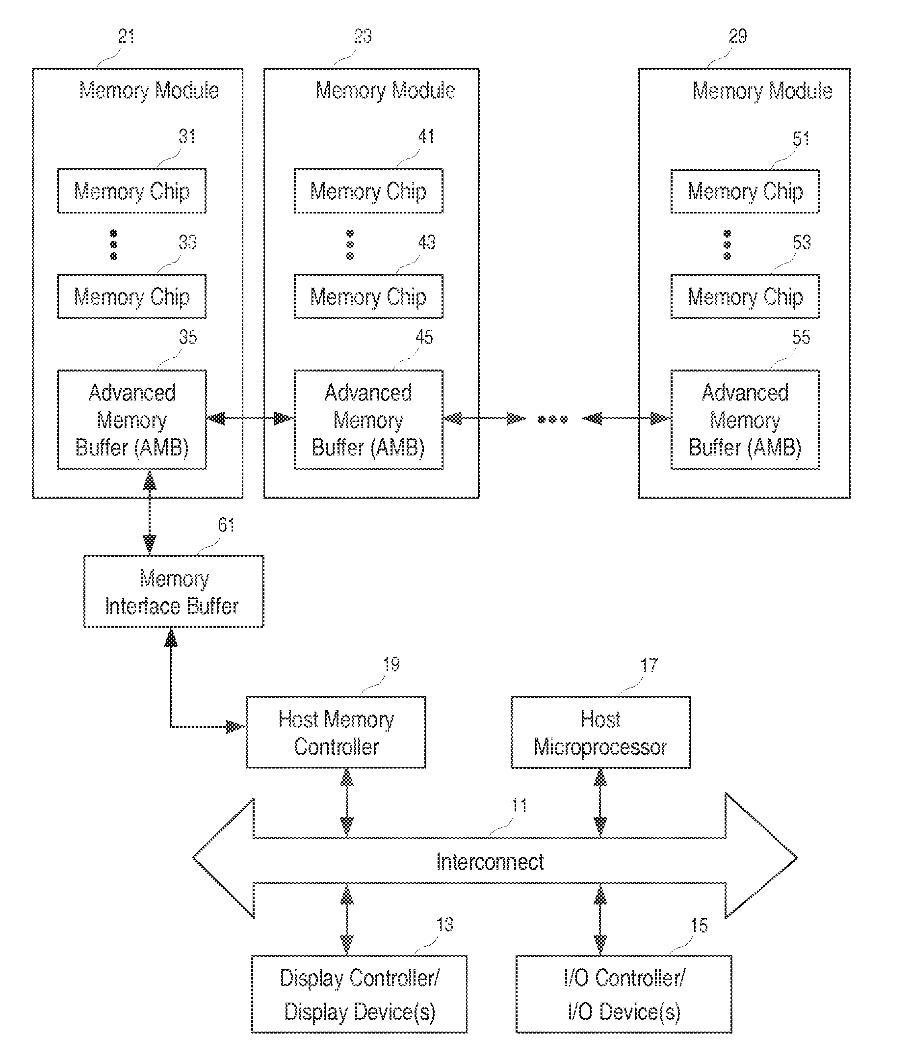
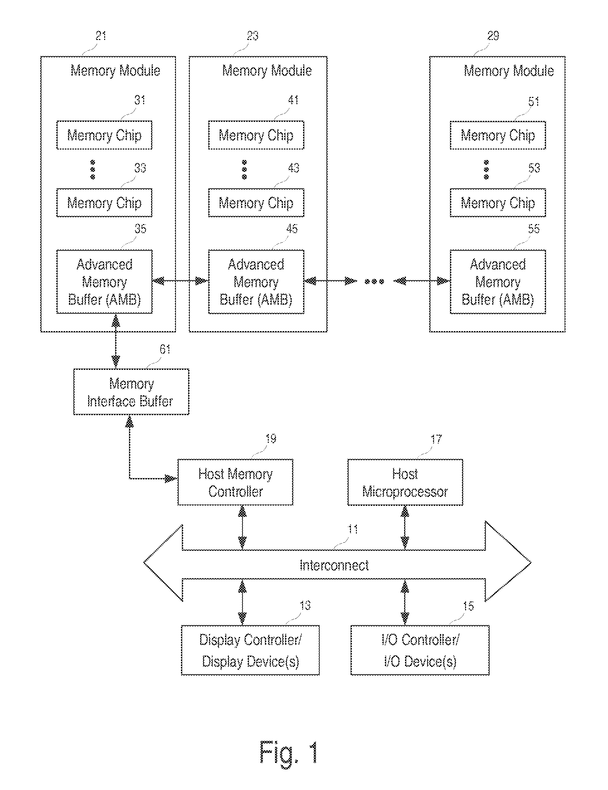
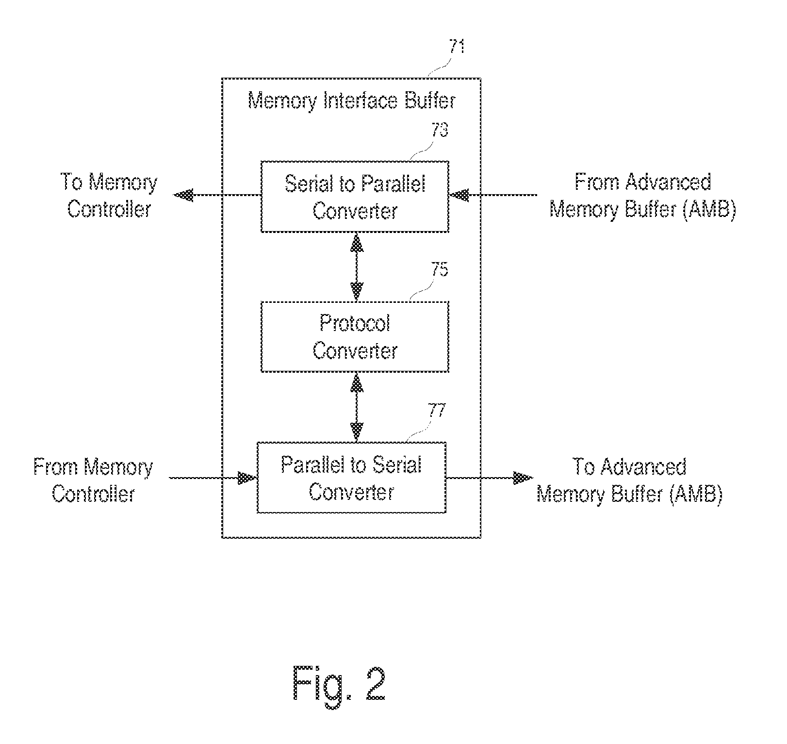
"The patent describes a memory interface that can connect a parallel memory bus and a serial memory bus. This interface includes a printed circuit board with a memory interface buffer chip, a memory bus, and a memory controller. The printed circuit board also includes a memory bus to connect the memory modules. The computer system includes a microprocessor chip, a core logic chip, and one or more non-fully buffered memory modules. The non-fully buffered memory modules are accessed via a parallel memory bus, while the fully buffered memory modules are accessed via a serial memory bus. The circuit includes a transceiver to bridge the parallel and serial memory buses and a protocol converter to translate control signals. The invention allows for efficient data transfer between different memory modules and improves overall performance of the computer system."

Problems solved by technology

When the number of modules in the channel increases, the channel performance decreases and thus limits the performance of the memory system.

Method used


Image

  • Memory interface to bridge memory buses
  • Memory interface to bridge memory buses
  • Memory interface to bridge memory buses

Examples


Embodiment Construction

[0039]The following description and drawings are illustrative of the invention and are not to be construed as limiting the invention. Numerous specific details are described to provide a thorough understanding of the present invention. However, in certain instances, well-known or conventional details are not described in order to avoid obscuring the description of the present invention. References to one or an embodiment in the present disclosure are not necessarily references to the same embodiment; and, such references mean at least one.

[0040]Fully Buffered—Dual-in-line Memory Modules (FB-DIMMs) are being developed to meet the increasing demand of memory capacity and bandwidth. FB-DIMM technology uses a memory controller that has an AMB interface to access FB-DIMMs. However, many current available memory controllers are capable of connecting to the conventional un-buffered or registered Dual Inline Memory Modules (DIMMs) but not to the FB-DIMMs, because of the lack of an AMB inter...


PUM


Abstract

A memory interface to bridge a parallel memory bus and a serial memory bus. One embodiment includes a printed circuit board, comprising: at least one memory interface buffer chip to connect an advanced memory buffer (AMB) interface and one or more non-fully buffered memory modules.

Description

CROSS REFERENCE TO RELATED APPLICATION[0001]This application is a continuation-in-part application of U.S. patent application Ser. No. 11 / 281,211, filed Nov. 16, 2005, and U.S. patent application Ser. No. 11 / 277,650 filed Mar. 28, 2006, the disclosure of which is incorporated herein by reference.FIELD OF THE TECHNOLOGY[0002]At least some embodiments of the invention relate to memory systems, and more specifically but not exclusively to memory systems with fully buffered memory modules.BACKGROUND[0003]Conventional memory systems use un-buffered or registered DIMMs that are connected by means of a stub bus, in which the memory modules are connected to a single channel. When the number of modules in the channel increases, the channel performance decreases and thus limits the performance of the memory system.[0004]To increase the performance of the dynamic random access memory (DRAM) system of a computer system, the technology of Fully Buffered Dual In-line Memory Module (FB-DIMM) has b...

Claims


Application Information

Patent Timeline
Patent Type & Authority Applications(United States)
IPC IPC(8): G11C5/06G06F13/00
CPCG11C5/04G11C29/02H05K1/181G11C29/022G11C29/028G11C29/021
Inventor YANG, HOWARDTAI, STEPHENSHAN, GANGWU, LARRY
Owner MONTAGE TECH HLDG CO LTD
Learn More