Touch panel, method for detecting touch input position, electro-optic device, and electronic device

a technology of touch input and position detection, applied in the field of touch panel, can solve the problems of spacer and glass substrate coming into contact, erroneous detection of spacer position, etc., and achieve the effect of preventing erroneous detection of touch input position and excellent reliability

Inactive Publication Date: 2007-07-19
SEIKO EPSON CORP
View PDF8 Cites 83 Cited by
  • Summary
  • Abstract
  • Description
  • Claims
  • Application Information

AI Technical Summary

Benefits of technology

[0033]According to this structure, because the electronic device includes the touch panel that makes it possible to preve...

Problems solved by technology

In the touch panel in the above described patent document, there is concern that, even when there is no touch input, a spacer and the glass substrate will come into contact due to flexion of the transparent resin film or the like.
Moreover, if the vicinity of a space...

Method used


Image

  • Touch panel, method for detecting touch input position, electro-optic device, and electronic device
  • Touch panel, method for detecting touch input position, electro-optic device, and electronic device
  • Touch panel, method for detecting touch input position, electro-optic device, and electronic device

Examples


first embodiment

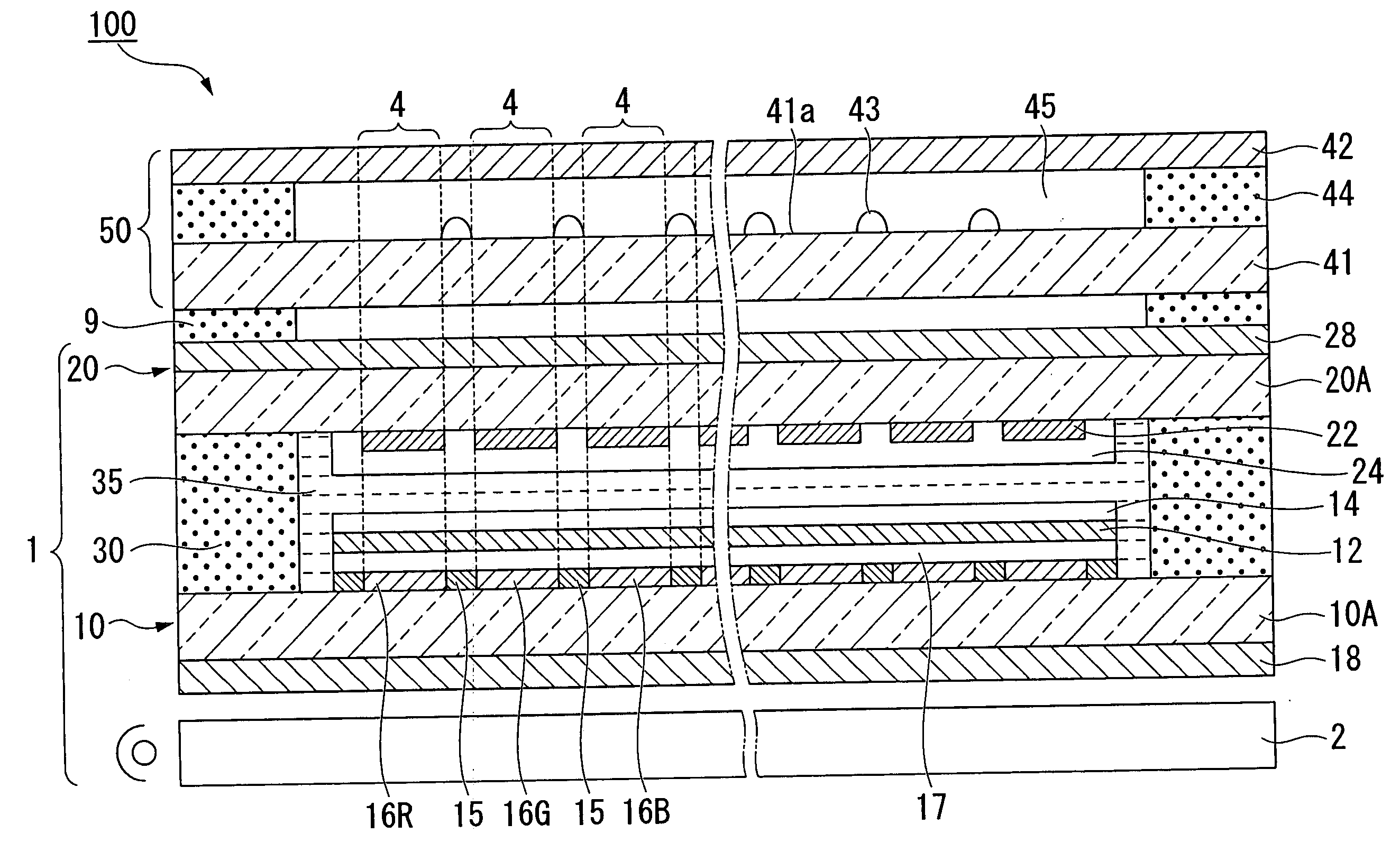
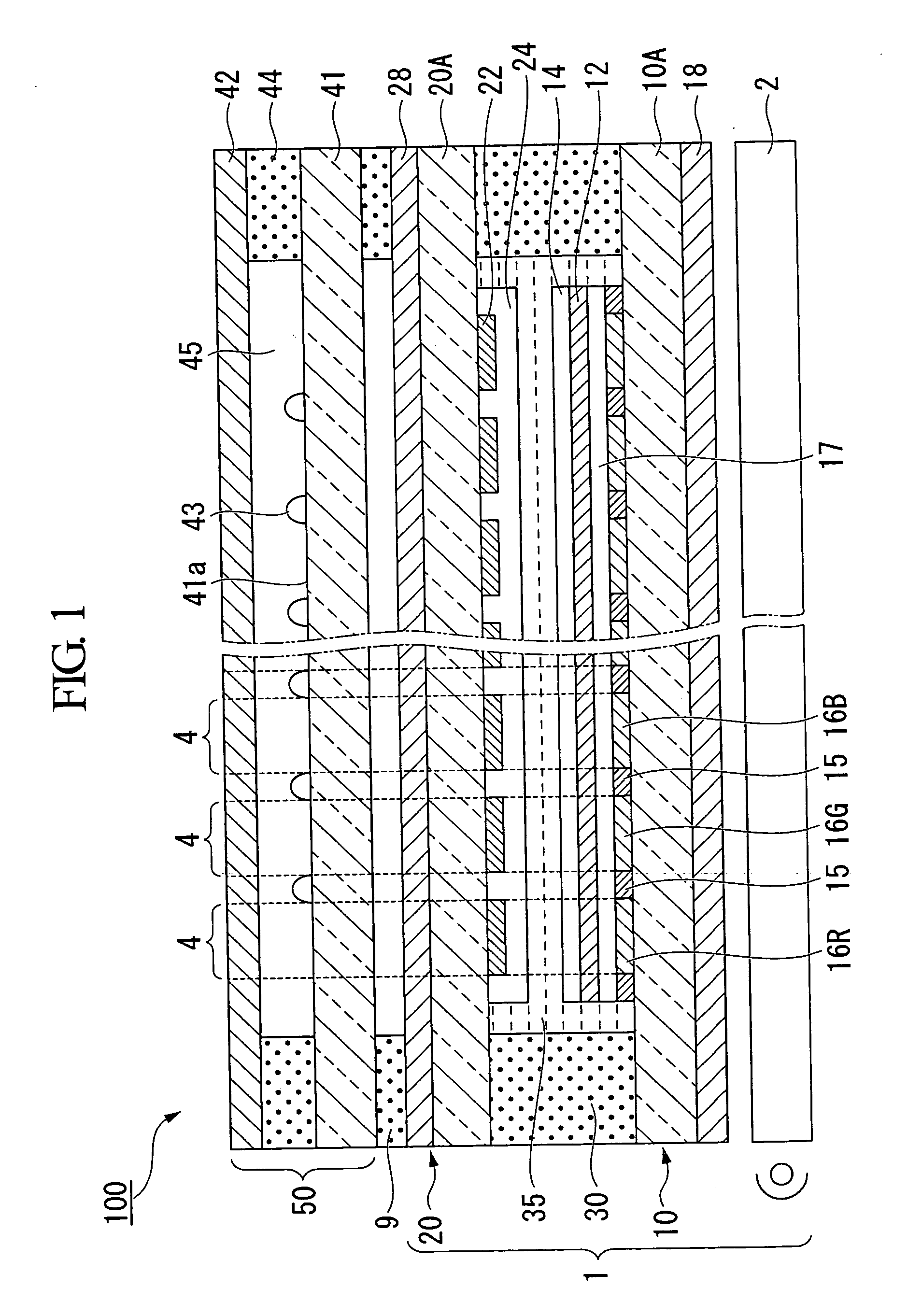
[0049]FIG. 1 is an explanatory view of an electro-optic device according to a first embodiment, and is a cross-sectional view taken along the line A-A in FIG. 2.

[0050]As shown in FIG. 1, in an electro-optic device 100 according to the first embodiment, a touch panel 50 is arranged on an image display side (i.e., a front side) of an image display device in the form of a liquid crystal device 1.

[0051]Liquid Crystal Device

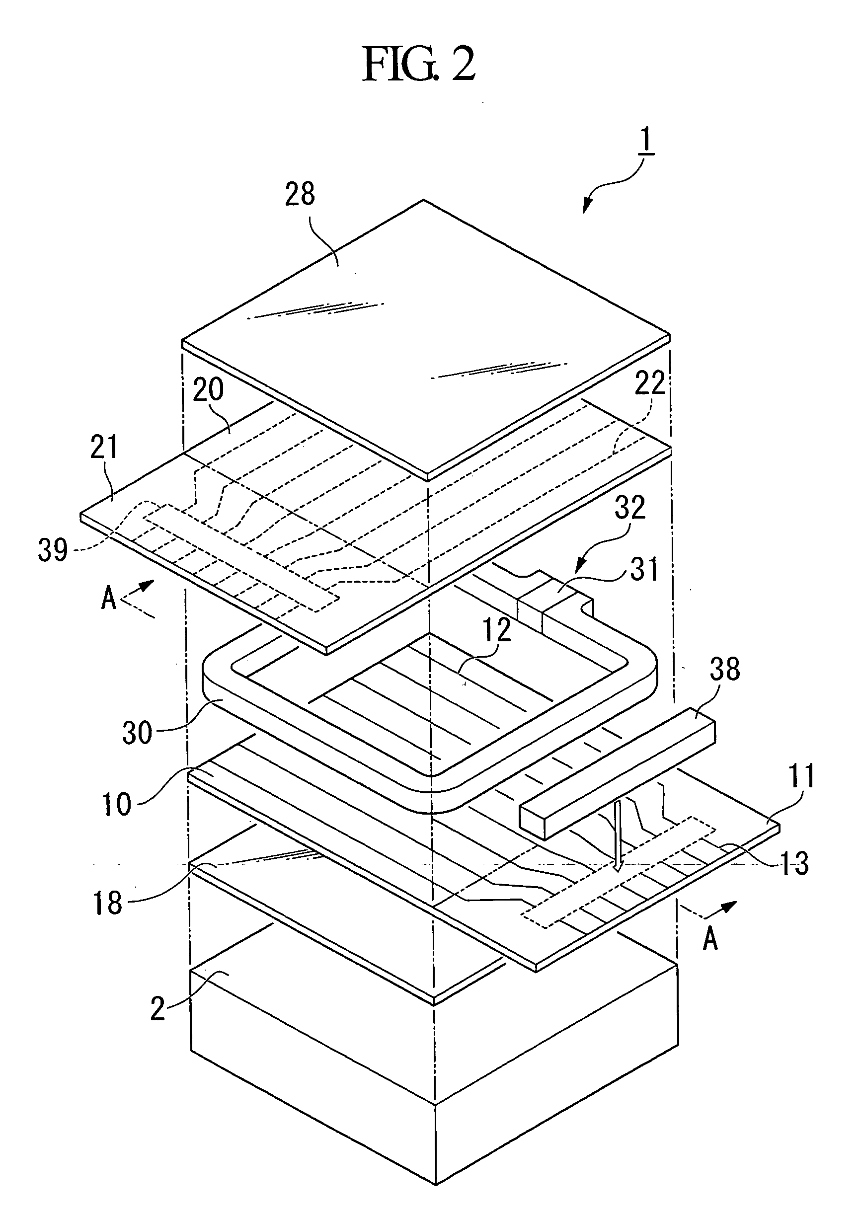
[0052]FIG. 2 is an exploded perspective view of a liquid crystal device.

[0053]In this embodiment, a passive matrix type of liquid crystal device is used as an example, however, it is also possible for this invention to be applied to an active matrix type of liquid crystal device.

[0054]In the liquid crystal device 1, a pair of substrates formed by a bottom substrate 10 and a top substrate 20 that are made of a transparent material such as glass are positioned facing each other.

[0055]Spacers (not shown) are arranged between the two substrates 10 and 20, and the space be...

second embodiment

[0211]FIG. 9 is an explanatory view of an electro-optic device according to a second embodiment and is a cross-sectional view taken along a line A-A in FIG. 2.

[0212]In the electro-optic device according to the second embodiment shown in FIG. 9, the polarization plate 28 on the image display side of the liquid crystal device 1 is arranged instead of the cover film of the first embodiment.

[0213]A detailed description of portions having the same structure as in the first embodiment is omitted.

[0214]In the second embodiment, a touch panel substrate 41 of a touch panel 50 is installed on an outer side of the top substrate 20 of the liquid crystal device 1.

[0215]The polarization plate 28 of the liquid crystal device 1 is arranged so as to face the touch input surface 41a of this touch panel substrate 41.

[0216]In this polarization plate 28, a polarization film obtained by doping polyvinyl alcohol (PVA) or the like with iodine is mounted on a base substrate made from cellulose triacetate (T...

third embodiment

[0221]FIG. 10 is an explanatory view of an electro-optic device according to a third embodiment and is a cross-sectional view taken along a line A-A in FIG. 2. In the electro-optic device according to the third embodiment shown in FIG. 10, the top substrate 20 of the liquid crystal device functions as a touch panel substrate.

[0222]A detailed description of portions having the same structure as in the first embodiment and second embodiment is omitted.

[0223]In the third embodiment, a transmitter, reflective array, and receiver of surface acoustic waves (none of which are shown) are arranged on a surface of the top substrate 20 of the liquid crystal device 1.

[0224]Spacers 43 are also arranged on the surface of the top substrate 20.

[0225]Moreover, in the same way as in the second embodiment, the polarization plate 28 is arranged so as to face the top portion substrate 20.

[0226]In this manner, in this embodiment, because the top portion substrate20 of the liquid crystal device 1 is confi...


PUM


Abstract

A touch panel includes: a touch panel substrate having an input surface; a cover film arranged separately from the input surface, and facing to the input surface; spacers extending upright from the touch panel substrate toward the cover film; a transmitter causing surface acoustic waves to be propagated on the input surface; a receiver measuring the surface acoustic waves propagated on the input surface; a memory storing, as reference values, measurement values of the surface acoustic waves when the cover film is not being pressed; and a determination section detecting, as touch input positions, positions at which a difference between the measurement values of the surface acoustic waves when the touch panel is being used and the reference values is significant.

Description

CROSS-REFERENCE TO RELATED APPLICATION[0001]This application claims priority from Japanese Patent Application No. 2006-009469, filed Jan. 18, 2006, the contents of which are incorporated herein by reference.BACKGROUND[0002]1. Technical Field[0003]The present invention relates to a touch panel, a method for detecting a touch input position thereof, an electro-optic device, and an electronic device.[0004]2. Related Art[0005]In recent years, in conjunction with the increasing use of small information electronic devices such as personal digital assistants (PDA) and palm top computers, liquid crystal devices having a touch panel mounted as an input device on the liquid crystal panel have become widely used.[0006]Of these, in ultrasonic surface acoustic wave type touch panels, a touch input position is detected utilizing the propensity of surface acoustic waves that are over the surface of a glass substrate to become attenuated at a touch input position.[0007]An example of this type of to...

Claims


Application Information

Patent Timeline
IPC IPC(8): G06F3/043
CPCG06F3/0436G06F3/0412G06F3/04166G02F1/13338G06F1/1643G06F3/03547
Inventor SAKURAI, SHINJITAGUCHI, SATOSHIFUNASAKA, TSUKASA
Owner SEIKO EPSON CORP
Why Eureka
Try Eureka