Semiconductor laser device, method for manufacturing the same and optical pickup apparatus

a laser device and semiconductor technology, applied in the direction of lasers, optical beam sources, semiconductor lasers, etc., can solve the problems of reducing the yield rate, affecting the downsizing process, and difficult to make the device small, so as to achieve the effect of a smooth surface and easy to obtain

Inactive Publication Date: 2007-07-19
SHARP KK
View PDF1 Cites 5 Cited by
  • Summary
  • Abstract
  • Description
  • Claims
  • Application Information

AI Technical Summary

Benefits of technology

[0056] According to the invention, the cap is formed by injecting resin into the mold. The mold is formed so as to have a rough surface, and a cap can be easily obtained which has an inner rough surface onl...

Problems solved by technology

Therefore, there is a possibility that the laser chip 8 fixed to the island portion 4 is heated via the island portion 4 having high thermal conductivity, which may cause a decrease of yield rate.
In the case of forming the fitting portions or engaging portions, there is a problem that it is difficult to make the device small and moisture or the like is easy to penetrate through a gap into the device.
However, in the case of fixing the cap and island using the adhesive, there is a need to make a region to apply the adhesive, and hence, th...

Method used


Image

  • Semiconductor laser device, method for manufacturing the same and optical pickup apparatus
  • Semiconductor laser device, method for manufacturing the same and optical pickup apparatus
  • Semiconductor laser device, method for manufacturing the same and optical pickup apparatus

Examples


Embodiment Construction

[0072] Now referring to the drawings, preferred embodiments of the invention are described below.

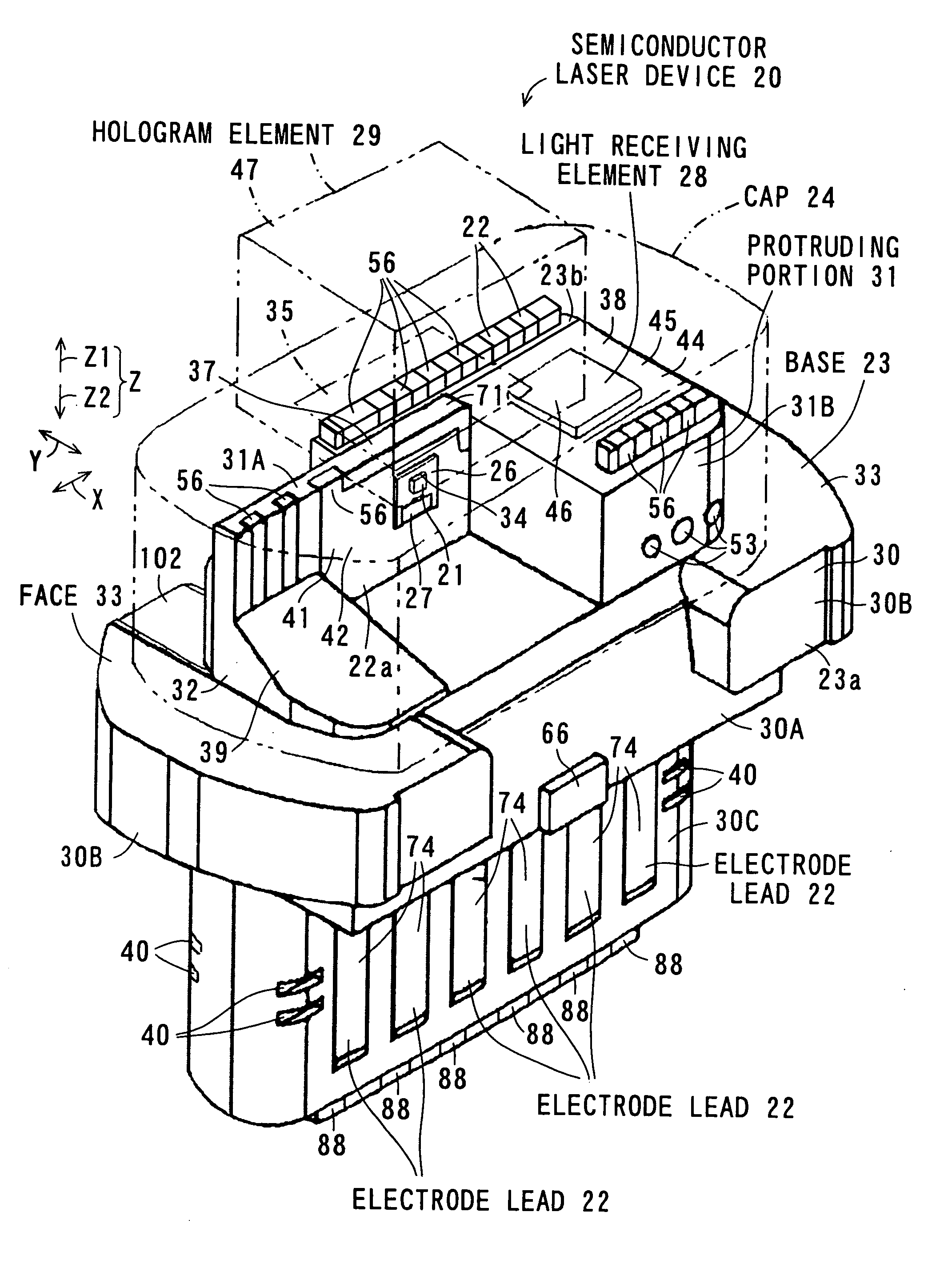
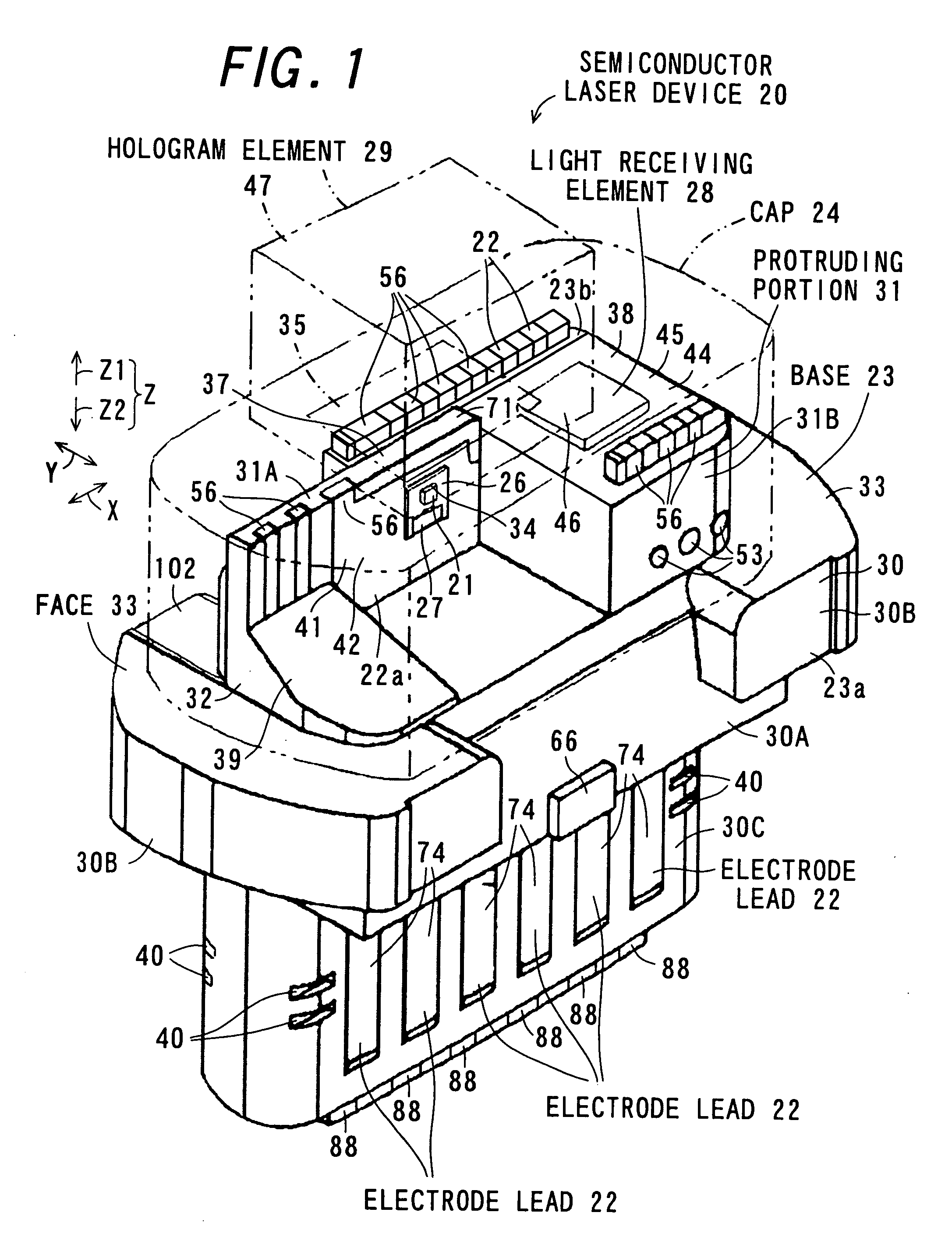
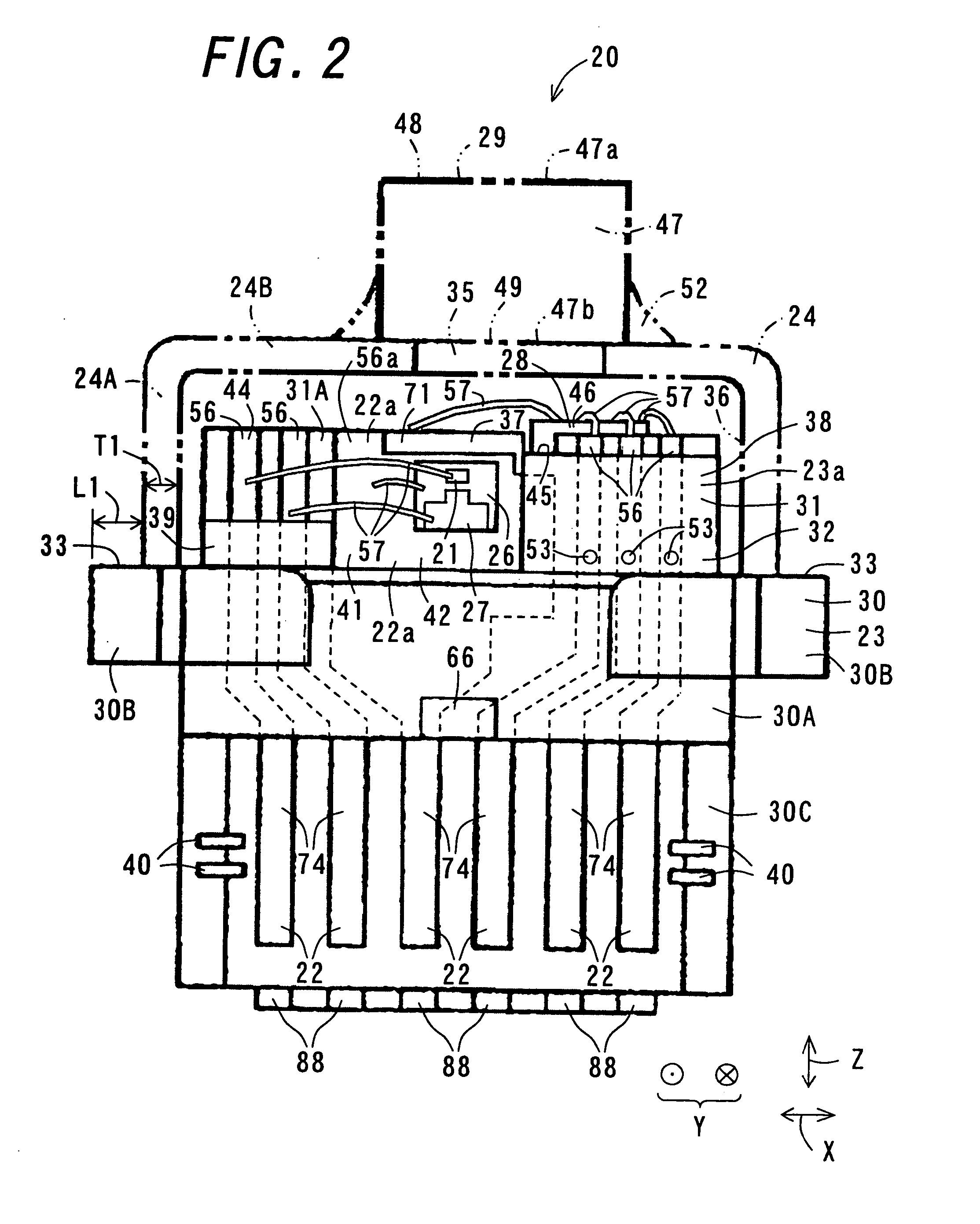
[0073]FIG. 1 is a perspective view illustrating a configuration of a semiconductor laser device 20 according to one embodiment of the invention. FIG. 2 is a front view illustrating the configuration of the semiconductor laser device 20, FIG. 3 is a rear view illustrating the configuration of the semiconductor laser device 20, FIG. 4 is a plan view illustrating the configuration of the semiconductor laser device 20, and FIG. 5 is a left side view illustrating the configuration of the semiconductor laser device 20. In FIGS. 1, 4 and 5, illustration of bonding wires 57 is omitted in order to prevent that the views become complicated.

[0074] The semiconductor laser device 20 comprises a semiconductor laser chip 21, a plurality of electrode leads 22, a base 23, and a cap 24. The semiconductor laser device 20 of the present embodiment further comprises a sub mount 26, a monitoring light recei...


PUM


Abstract

A semiconductor laser chip is mounted on one surface of an electrode lead for chip mounting having a heat release region for releasing heat around the semiconductor laser chip. Therefore, it is possible to release heat of the semiconductor laser chip to the chip mounting lead and release the heat from the heat release region, thereby suppressing increase of a temperature of the semiconductor laser chip and suppressing shortening of life of the semiconductor laser chip.

Description

CROSS-REFERENCE TO RELATED APPLICATION [0001] This application claims priority to Japanese Patent Application No. JP 2006-11694, which was filed on Jan. 19, 2006, the contents of which, are incorporated herein by reference, in their entirety. BACKGROUND OF THE INVENTION [0002] 1. Field of the Invention [0003] The present invention relates to a semiconductor laser device that is equipped with a semiconductor laser chip and is used as, for example, a light source of an optical pickup apparatus for an optical disk system, and also relates to a method for manufacturing the semiconductor laser device. [0004] 2. Description of the Related Art [0005]FIG. 14 is a perspective view illustrating a configuration of a related art semiconductor laser device 1. The semiconductor laser device 1 disclosed in Japanese Unexamined Patent Publication JP-A 2002-232059 comprises: an island portion 4 that is a component made of metal including a reference face 2 and a block portion 3 protruding in a direct...

Claims


Application Information

Patent Timeline
IPC IPC(8): H01S3/04G11B7/125H01S5/0232
CPCH01S5/02208H01S5/02244H01S5/02248H01S5/02469H01L2224/48091H01S5/02476H01L2924/00014H01S5/0231H01S5/02325H01S5/0232
Inventor HAMAOKA, OSAMU
Owner SHARP KK
Why Eureka
Try Eureka