Microelectronic device with mixed dielectric

a technology of mixed dielectric and microelectronic device, which is applied in the direction of printed circuit aspects, high frequency circuit adaptation, printed electric component incorporation, etc., can solve the problems of inability to design a die with inability to achieve high density bonding pad, etc., to achieve the effect of reducing the capacitive parasitic of the conductor

Inactive Publication Date: 2007-07-26
GLOBALFOUNDRIES INC
View PDF10 Cites 7 Cited by
  • Summary
  • Abstract
  • Description
  • Claims
  • Application Information

AI Technical Summary

Benefits of technology

[0007] It is another object of this invention to provide a low permittivity material adjacent to or in contact with a portion of a conductor to reduce capacitive parasitic of the conductor, resulting in a substantially higher characteristic impedance of the conductor during operation of a microelectronic device of which it is a part.

Problems solved by technology

This design is not practical for dies with high density bonding pads and is against the trend of smaller die pad pitch for advance technologies (almost all new applications are migrating in the direction of smaller bonding pad pitch to save die area and lower cost).
Changing to a lower permittivity dielectric package carrier may solve this characteristic impedance issue, but may introduce new electrical problems to the power structure and undesirably alter the loss, mechanical, density and thermal characteristics as compared to a ceramic substrate.

Method used


Image

  • Microelectronic device with mixed dielectric
  • Microelectronic device with mixed dielectric
  • Microelectronic device with mixed dielectric

Examples


Embodiment Construction

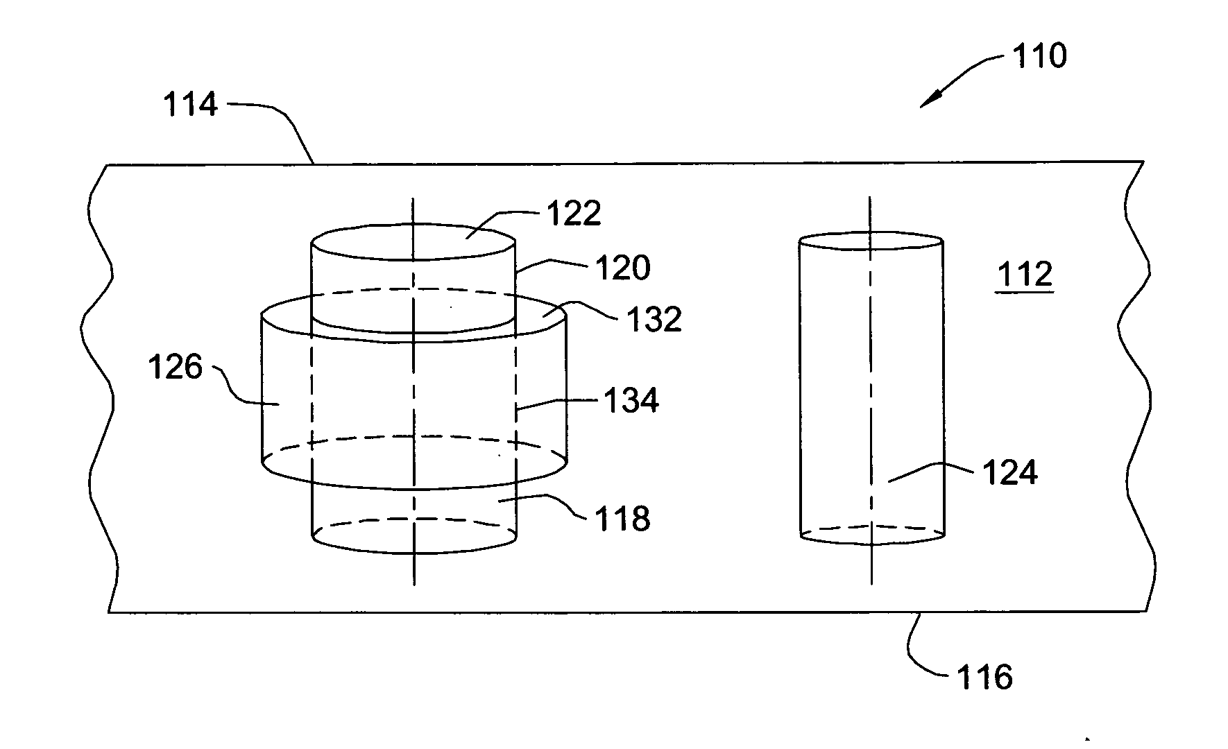
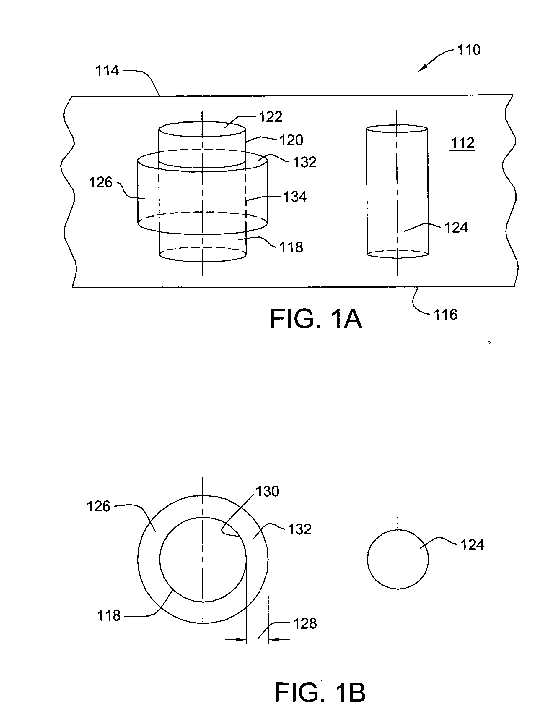
[0018] A much enlarged view in elevation of a portion of a microelectronic device 110 for use with a semiconductor chip (not shown) illustrating one embodiment of the present invention is shown in FIG. 1A. Microelectronic device 110 includes a dielectric substrate 112 having first and second surfaces, 114 and 116, respectively. A first component 118 is located in dielectric substrate 112 between first surface 114 and second surface 116 of the dielectric substrate, having a first interface 120 and a second interface 122. A second component 124 is located in dielectric substrate 112 and spaced relative to first component 118. The spacing between first and second components can be from about 150 um to about 800 um. A first low permittivity material 126 having a predetermined thickness 128 (see FIG. 1B) includes a first surface 130 and a second surface 132, the first surface of the low permittivity material is adjacent to or in contact with a first portion 134 of first interface 120 of ...


PUM


Abstract

A microelectronic device and method of making the microelectronic device is provided. A dielectric substrate having first and second surfaces is provided. A first component, located in the dielectric substrate between the first and second surfaces of the dielectric substrate is formed. The first component includes a first interface and a second interface. A second component located in the dielectric substrate and spaced relative to the first component is formed, and a first low permittivity material is formed having a predetermined thickness and a first and second surface, the first surface of the low permittivity material is adjacent to or in contact with a first portion of the first interface of the first component. The first low permittivity material substantially reduces capacitive parasitics of the first component, resulting in a substantially higher characteristic impedance of the first component during operation of the microelectronic device.

Description

FIELD OF THE INVENTION [0001] The invention relates to a microelectronic device for use in packaging semiconductors having mixed dielectric materials therein, more particularly to such packages where some of the conductors have increased characteristic impedance as a result of the mixed dielectric positioning within the package. A method of making the microelectronic device is also provided. BACKGROUND OF THE INVENTION [0002] In the electronics industry low signal impedance in interconnect structures, for example, in vias, is a concern. [0003] In a microelectronic device, such as a ceramic flip-chip package, electrical performance of vias is becoming more and more significant to the overall signal integrity when the signal speed or frequency moves higher, as well as the die bonding pad pitch is reduced. This is mainly due to the discontinuity or the lower characteristic impedance of the vias. For high speed and RF signal applications, interconnects (traces: horizontal structures, vi...

Claims


Application Information

Patent Timeline
Patent Type & Authority Applications(United States)
IPC IPC(8): H05K1/16
CPCH01L23/15H01L23/49827H01L23/49894H01L23/66H01L2924/3011H05K1/024H05K1/0306H01L2924/0002H05K1/115H05K2201/0187H05K2201/0792H05K2201/09581H01L2924/00
Inventor DING, HANYIWELCH, BRIAN P.
Owner GLOBALFOUNDRIES INC
Why Eureka
Try Eureka