Arrays of microcavity plasma devices with dielectric encapsulated electrodes

a plasma device and dielectric encapsulation technology, applied in the manufacture of electrode systems, electric discharge tubes/lamps, nuclear elements, etc., can solve the problems of high cost materials, short life of early microcavity plasma devices, and inability to meet the requirements of microcavity plasma devices, etc., and achieve the effect of cheap production

Active Publication Date: 2007-07-26
THE BOARD OF TRUSTEES OF THE UNIV OF ILLINOIS
View PDF39 Cites 50 Cited by
  • Summary
  • Abstract
  • Description
  • Claims
  • Application Information

AI Technical Summary

Benefits of technology

[0012] The invention concerns microcavity plasma devices and arrays with thin foil metal electrodes protected by metal oxide dielectric. Devices of the invention are amenable to mass production techniques, and may, for example, be fabricated by roll to roll processing. Exemplary devices of the invention are flexible. Embodiments of the invention provide for large arrays of microcavity plasma devices that can be made inexpensively.

Problems solved by technology

In addition, the efficiency of a microcavity plasma device exceeds that of a conventional plasma display panel, such as those used in high definition televisions.
Early microcavity plasma devices exhibited short lifetimes because of sputtering that damaged metal electrodes used in the early, DC-driven devices.
Polycrystalline silicon and tungsten electrodes extend lifetime but are higher cost materials and difficult to fabricate with present techniques.

Method used


Image

  • Arrays of microcavity plasma devices with dielectric encapsulated electrodes
  • Arrays of microcavity plasma devices with dielectric encapsulated electrodes
  • Arrays of microcavity plasma devices with dielectric encapsulated electrodes

Examples


Embodiment Construction

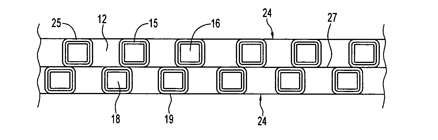
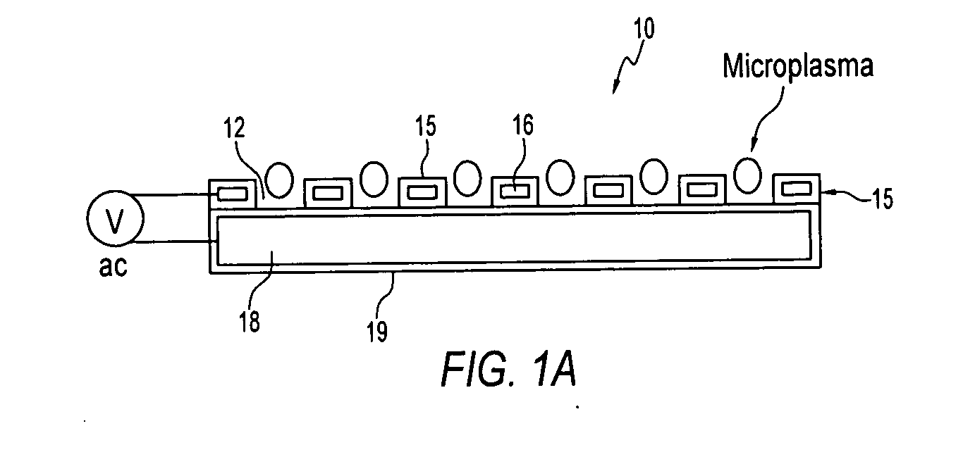
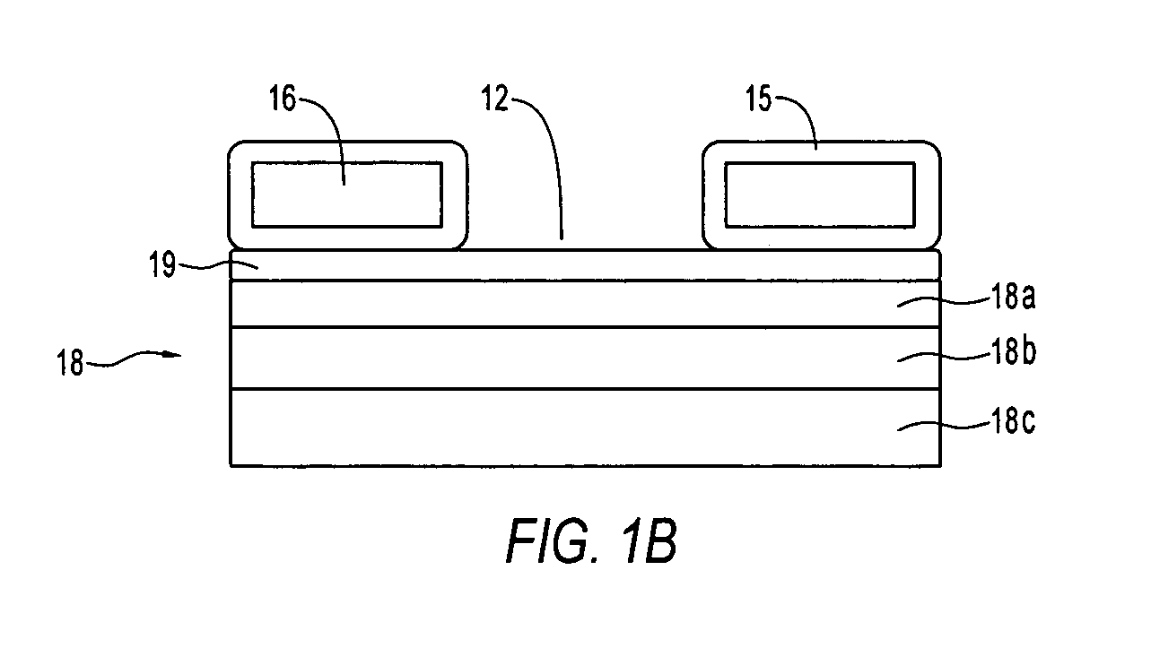
[0027] The invention concerns microcavity plasma devices and arrays of devices in which thin foil metal electrodes are protected by a metal oxide dielectric. Devices of the invention are amenable to mass production techniques, and may, for example, be fabricated by roll to roll processing. Exemplary devices of the invention are flexible. Embodiments of the invention provide for large arrays of microcavity plasma devices that can be made inexpensively.

[0028] The structure of preferred embodiment microcavity plasma devices of the invention is based upon thin foils of metal that are available or can be produced in arbitrary lengths, such as on rolls. In a device of the invention, a pattern of microcavities is produced in a metal foil. Oxide is subsequently grown on the foil, including within the microcavities, to define oxide encapsulated microcavities (in which the plasma is to be produced). The oxide protects the microcavity and electrically isolates the foil, which forms a first el...


PUM

PropertyMeasurementUnit
diameteraaaaaaaaaa
diameteraaaaaaaaaa
pressuresaaaaaaaaaa

Abstract

The invention concerns microcavity plasma devices and arrays with thin foil metal electrodes protected by metal oxide dielectric. Devices of the invention are amenable to mass production techniques, and may, for example, be fabricated by roll to roll processing. Exemplary devices of the invention are flexible. Embodiments of the invention provide for large arrays of microcavity plasma devices that can be made inexpensively. The structure of preferred embodiment microcavity plasma devices of the invention is based upon thin foils of metal that are available or can be produced in arbitrary lengths, such as on rolls. In a device of the invention, a pattern of microcavities is produced in a metal foil. Oxide is subsequently grown on the foil and within the microcavities (where plasma is to be produced) to protect the microcavity and electrically isolate the foil. A second metal foil is also encapsulated with oxide and is bonded to the first encapsulated foil. For preferred embodiment microcavity plasma device arrays of the invention, no particular alignment is necessary during bonding of the two encapsulated foils. A thin glass layer or vacuum packaging, for example, is able to seal the discharge medium into the array.

Description

PRIORITY CLAIM AND REFERENCE TO RELATED APPLICATION [0001] This application claims priority under 35 U.S.C. §119 from provisional application Ser. 60 / 699,475, filed Jul. 15, 2005, is a continuation-in-part of and claims priority under 35 U.S.C. §120 from U.S. application Ser. No. 10 / 958,174, filed Oct. 4, 2004, and is a continuation-in-part of and claims priority under U.S.C. §120 of U.S. application Ser. No. 10 / 958,175, filed Oct. 4, 2004 entitled “Metal / Dielectric Multilayer Microdischarge Devices and Arrays”.STATEMENT OF GOVERNMENT INTEREST [0002] This invention was made with Government assistance under U.S. Air Force Office of Scientific Research grant No. F49620-03-1-0391. The Government has certain rights in this invention.FIELD OF THE INVENTION [0003] The invention is in the field of microcavity plasma devices, also known as microdischarge devices or microplasma devices. BACKGROUND [0004] Microcavity plasma devices have several distinct advantages over conventional discharges...

Claims


Application Information

Patent Timeline
Patent Type & Authority Applications(United States)
IPC IPC(8): H01J61/04H01J17/04
CPCG21F1/106H01J9/248H01J61/76H01J61/305H01J17/04
Inventor EDEN, J. GARYPARK, SUNG-JIN
Owner THE BOARD OF TRUSTEES OF THE UNIV OF ILLINOIS
Why Eureka
Try Eureka