
New aperture design for improving critical dimension accuracy and electron beam lithography throughput

a technology of electron beam lithography and aperture design, which is applied in the field of new aperture design for improving critical dimension accuracy and electron beam lithography, can solve the problems of affecting the throughput of e-beam lithography, difficult to align different positions of the shape, and poor critical dimension accuracy

Inactive Publication Date: 2007-07-26
TAIWAN SEMICON MFG CO LTD
View PDF1 Cites 4 Cited by
  • Summary
  • Abstract
  • Description
  • Claims
  • Application Information

AI Technical Summary

Problems solved by technology

However, the requirement of multiple shots to create these patterns impacts the throughput of e-beam lithography, because multiple shots require a longer period of time to write.
In addition, multiple shots make it difficult to align different positions of the shape.
But as a result of the bias adjustment, the accuracy of critical dimension suffers.

Method used


Image

  • New aperture design for improving critical dimension accuracy and electron beam lithography throughput
  • New aperture design for improving critical dimension accuracy and electron beam lithography throughput
  • New aperture design for improving critical dimension accuracy and electron beam lithography throughput

Examples


Embodiment Construction

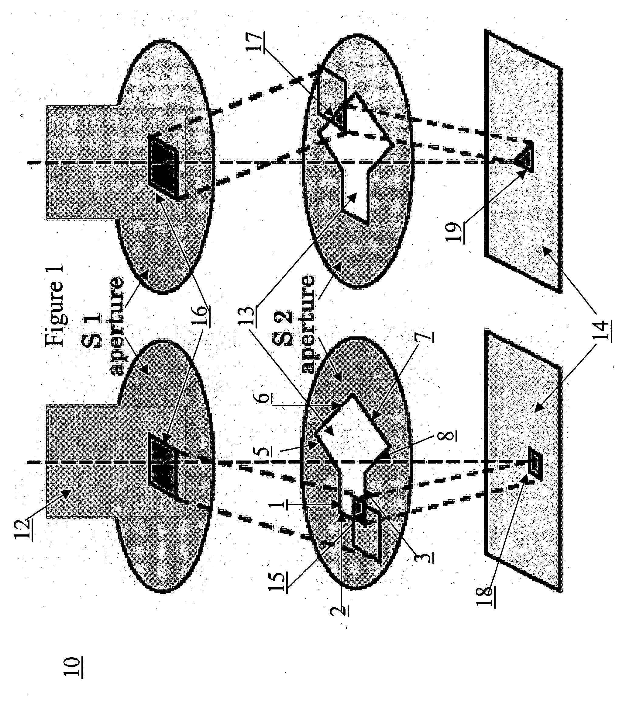
[0017]FIG. 1 is a diagram of an aperture design that requires multiple shots for creating a pattern on a reticle. As shown in FIG. 1, aperture design 10 comprises two apertures: S1 and S2. Aperture S1 has a rectangular shape 16, while aperture S2 has a shape 13 that composes three edges 1, 2, and 3 and four bevels 5, 6, 7, and 8. Horizontal edges 1 and 3 meet vertical edge 2 at a 90 degree angle. Bevels 5 and 8 meet horizontal edges 1 and 3 respectively at an angle greater than 90 degrees, while bevels 6 and 7 meet each other at an angle less than 90 degrees.

[0018] When e-beam 12 is focused towards reticle surface 14, the beam passes through the rectangular shape 16 of aperture S1 and is projected onto a portion of shape 13 of aperture S2. Consequently, the e-beam passes through the portion of shape 13 of aperture S2 resulting in an exposure of an overlapped portion 15 to the reticle surface 14. The overlapped portion 15 comprises an upper right corner of rectangular shape 16 and a...


PUM

PropertyMeasurementUnit
angleaaaaaaaaaa
angleaaaaaaaaaa
90 degree angleaaaaaaaaaa

Abstract

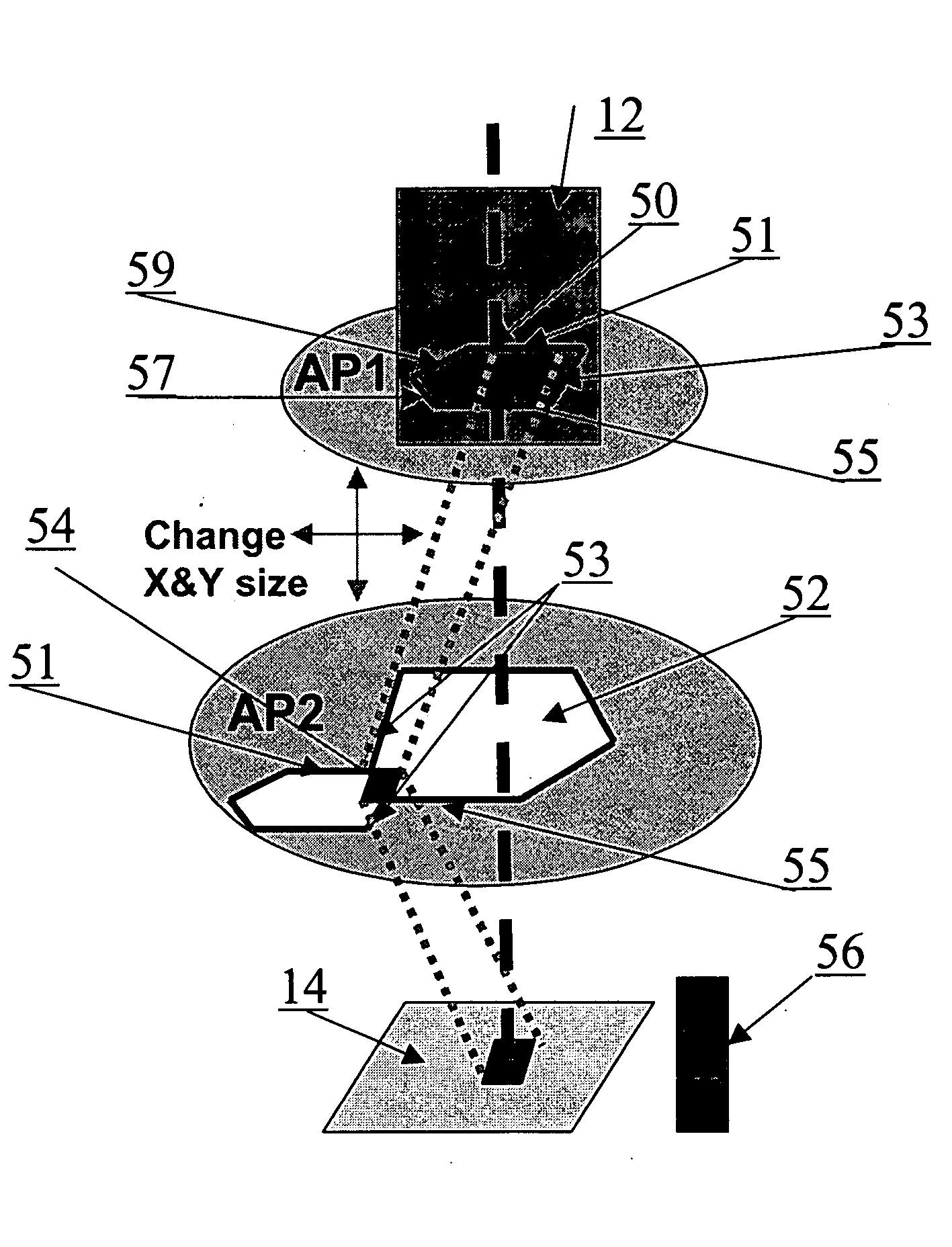
Disclosed is an improved aperture design for improving critical dimension accuracy and electron beam lithography. A pattern may be created on a reticle by passing an electron beam through a first aperture having a first shape comprising an upper horizontal edge, a lower horizontal edge, a vertical edge, an upper bevel, and a lower bevel, wherein a portion of the electron beam is projected onto a second aperture. The portion of the electronic beam is passed through the second aperture having a second shape, wherein the second shape is the first shape rotated horizontally by 180 degrees, and an overlapped portion of the first and second aperture is exposed on a surface of the reticle to create a pattern.

Description

BACKGROUND [0001] The present disclosure relates in general to semiconductor manufacturing technology, and more particularly, the present disclosure relates to beam lithography in semiconductor manufacturing technology. The present disclosure also relates to an improved aperture design for improving accuracy of critical dimension of an angle line and throughput of electron beam lithography. [0002] In semiconductor manufacturing technology, electron beam (e-beam) lithography is commonly used to create a complex pattern on a reticle. Generally, electrons from electron source are accelerated and focused in the shape of a beam toward the reticle. The electron beam is scanned in the desired pattern across an e-beam resist on the reticle surface. The e-beam resist may be a positive-tone poly or a chemically amplified resist. [0003] During e-beam lithography, multiple shots are required in order to create a pattern on the reticle. A shot is produced when the e-beam passes through a plurali...

Claims


Application Information

Patent Timeline
Patent Type & Authority Applications(United States)
IPC IPC(8): G03C5/00G06Q40/00G03F1/00
CPCB82Y10/00B82Y40/00H01J37/3174G03F7/2063G06Q40/00G03F1/78
Inventor CHEN, CHIA-JENLEE, HSIN-CHANGHSIEH, HUNG CHANG
Owner TAIWAN SEMICON MFG CO LTD
Learn More