Patterned SOI by oxygen implantation and annealing

a technology of oxygen implantation and annealing, applied in the direction of basic electric elements, electrical apparatus, semiconductor devices, etc., can solve problems such as fabrication challenges

Inactive Publication Date: 2005-01-25
GLOBALFOUNDRIES INC
View PDF26 Cites 36 Cited by
  • Summary
  • Abstract
  • Description
  • Claims
  • Application Information

AI Technical Summary

Benefits of technology

Another object of the present invention is to provide a method of forming at least one patterned SOI region within a Si-containing or SOI-containing substrate which maintains a substantially smooth surface topology between the patterned and unpatterned regions.
A further object of the present invention is to provide a method of forming at least one patterned SOI region within a Si-containing or SOI-containing substrate wherein the method essentially controls and substantially eliminates crystallographic defects at the edge of the mask used during the ion implantation to create the patterned regions.
A yet further object of the present invention is to provide a method of forming at least one patterned SOI region within a Si-containing or SOI-containing substrate wherein the method essentially controls and eliminates crystal defects between the nearby oxide islands, i.e., between the discrete buried oxide (BOX) regions.

Problems solved by technology

Despite this need, there are many challenges in fabricating patterned SOI regions within a Si or SOI-containing substrate.

Method used


Image

  • Patterned SOI by oxygen implantation and annealing
  • Patterned SOI by oxygen implantation and annealing
  • Patterned SOI by oxygen implantation and annealing

Examples


Embodiment Construction

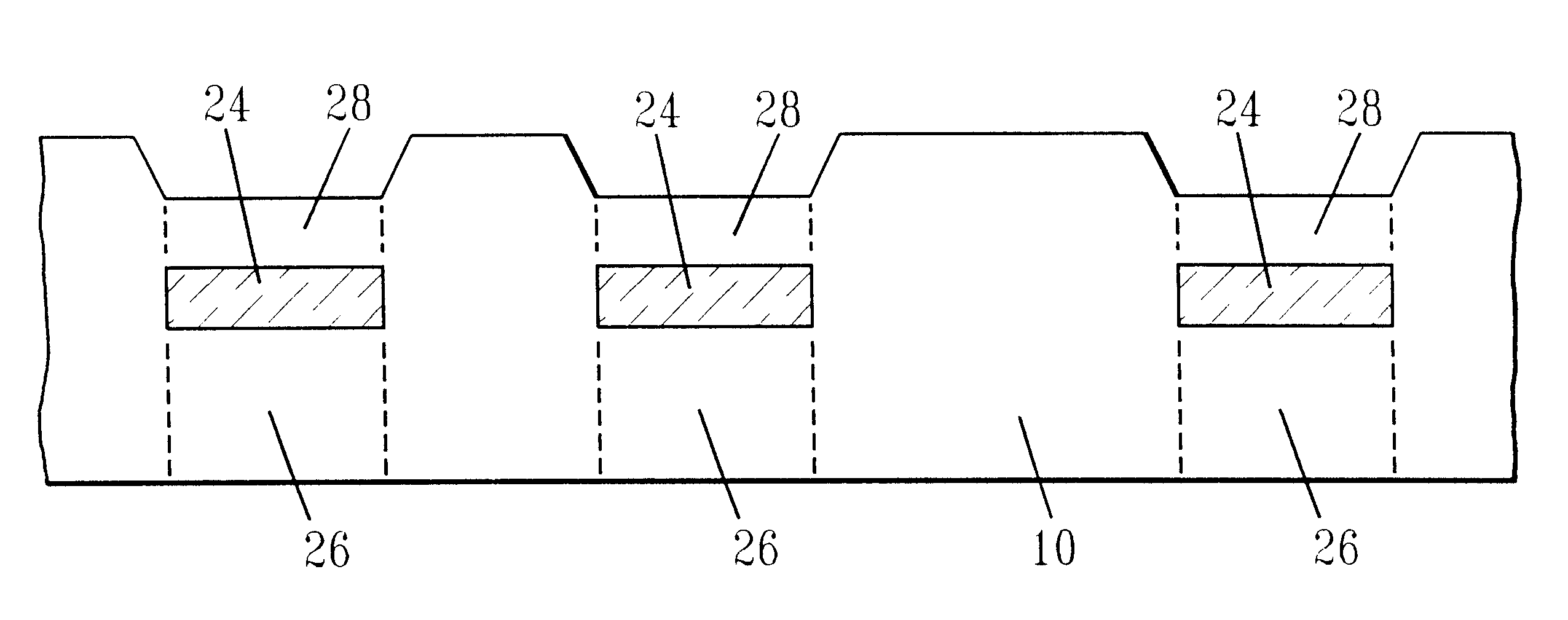
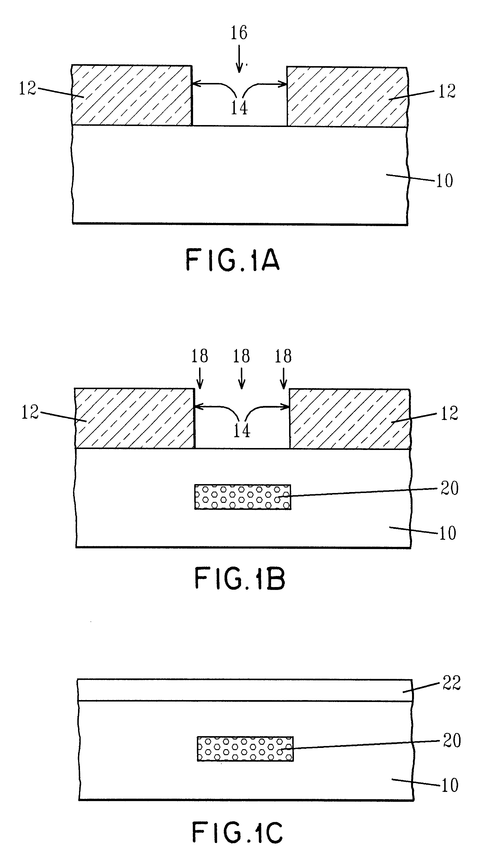
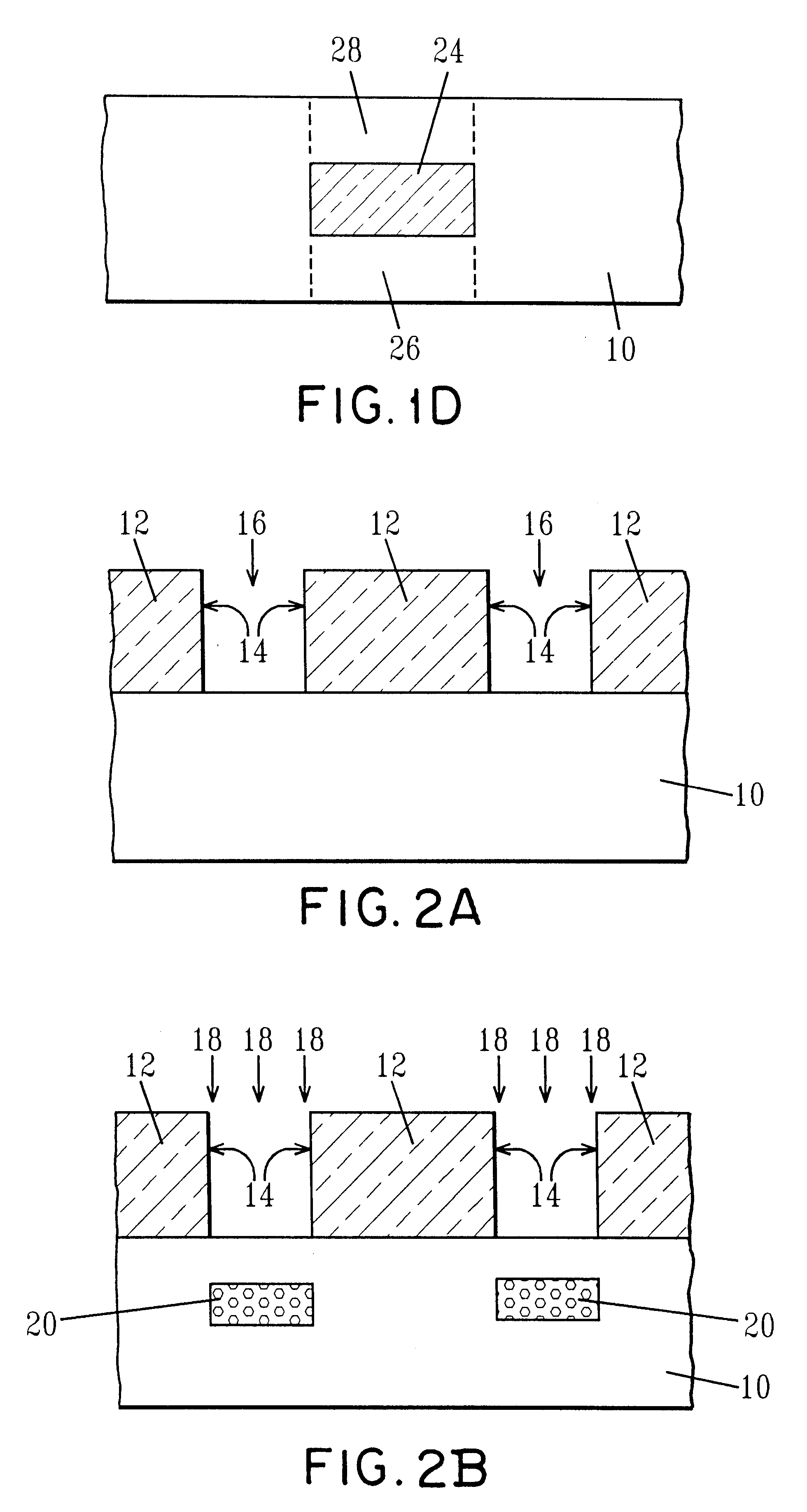
The present invention which relates to a method for providing a highly uniform sub-0.25 μm patterned SOI substrate containing discrete buried oxide regions will now be described in greater detail by referring to the drawings that accompany the present application. It is noted that like and / or corresponding elements in the drawings are referred to by like reference numerals.

Reference is first made to FIGS. 1A-1D which show cross-sectional views of the inventive patterned SOI substrate through various processing steps of the present invention. Specifically, FIG. 1A provides an illustration of an initial structure of the present invention. The initial structure shown in FIG. 1A comprises Si-containing substrate 10 having patterned dielectric mask 12 formed on a surface thereof. In accordance with the present invention, patterned dielectric mask 12 includes vertical or inclined edges 14 that define boundaries for at least one opening 16 which exposes a portion of the Si-containing subst...


PUM


Abstract

Methods for forming a patterned SOI region in a Si-containing substrate are provided which has geometries of about 0.25 μm or less. The methods disclose each utilize a patterned dielectric mask that includes at least one opening having a size of about 0.25 μm or less which exposes a portion of a Si-containing substrate. Oxygen ions are implanted through the opening using at least a base ion implantation process which is carried out at an oxygen beam energy of about 120 keV or less and an oxygen dosage of about 4E17 cm−2 or less. These conditions minimize erosion of the vertical edges of the patterned dielectric mask and minimize formation of lateral straggles.

Description

FIELD OF THE INVENTIONThe present invention relates to silicon-on-insulator (SOI) substrates for use in the semiconductor industry for fabricating integrated circuits (ICs), and more particularly to a method of forming highly uniform patterned SOI regions within a Si-containing substrate including a preformed SOI substrate, that has geometries of less than about 0.25 μm. SOI-containing substrates may contain a single or multiple buried oxide (BOX) regions in blanket or patterned fashion. High quality buried oxide (BOX) regions are also formed in the present invention.BACKGROUND OF THE INVENTIONSeparation by implantation of oxygen (SIMOX) is a technique used in the semiconductor industry in fabricating SOI substrates that can be used in the manufacturing of ICs. SIMOX typically involves using high-energy ions to implant a large dose of oxygen ions beneath the surface of a bulk Si-containing wafer. Upon high-temperature annealing, the implanted oxygen ions form a continuous BOX region...

Claims


Application Information

Patent Timeline
Patent Type & Authority Patents(United States)
IPC IPC(8): H01L21/762H01L21/70
CPCH01L21/76243
Inventor FOGEL, KEITH E.HAKEY, MARK C.HOLMES, STEVEN J.SADANA, DEVENDRA K.SHAHIDI, GHAVAM G.
Owner GLOBALFOUNDRIES INC
Why Eureka
Try Eureka