Method and apparatus for probing at arbitrary locations within an inaccessible array of leads the solder balls or pins actually connecting a VLSI IC package to a substrate or socket

a technology of vlsi ic and array of leads, which is applied in the direction of electrical testing, measurement devices, instruments, etc., can solve the problems of difficulty in electrical testing and troubleshooting, pins are frequently not accessible, and the state of affairs is by no means guaranteed

Inactive Publication Date: 2007-08-02
AGILENT TECH INC
View PDF2 Cites 4 Cited by
  • Summary
  • Abstract
  • Description
  • Claims
  • Application Information

AI Technical Summary

Benefits of technology

[0014] The shape of a contact that touches a solder ball for electrical connection thereto may be a concavity, a convex region, a flat region, or one of the preceding with some sort of detent, such as a notch. In the case of a flat region, it's edge might be parallel to the line of progressive insertion, or at an angle thereto. In any event, the width of the probe at the contact(s) is slightly wider than the narrowest distance between two adjacent solder balls and through which the line of advance requires it to pass. It is this interference that produces the compressive warping that allows the probe to pass in and out, while at the same time urging the contact(s) into the solder ball(s) that they may be touching. Regions of the probe that do not carry contacts are narrow enough to slide freely between adjacent solder balls.

Problems solved by technology

Alas, this venerable cost effective and efficient style of mechanical mounting and electrical interconnection between an IC and its host PCA presents a difficulty for electrical testing and troubleshooting.
The trouble arises because the tasks of testing and troubleshooting generally require the probing of the signals at the pins of the IC, and those pins are frequently not accessible.
It may happen that a pin of interest is accessible from the back side of the PCA, but this state of affairs is by no means assured.
When this occurs, both the ‘front side’ and ‘back side’ pads of even a Ball Grid Array having all or mostly through vias are covered by those parts, and no conventional actual electrical access to their pads is possible.
Unfortunately, the very increase in complexity and functionality possessed by those parts needing BGA style mounting is also accompanied by an increased need for testing during system turn-on and troubleshooting.
Certain critical signals can often be deliberately made available as accessible test points during the layout process, but a wholesale leading of all pads of a BGA to such test points is undesirable, both from an efficient use of board space, and also from an electrical perspective: high speed signal are often conveyed over transmission lines, and the needed ‘tee’ connection is an unwanted stub that can distort fast signals and have a severe impact on performance.
The task or troubleshooting a malfunctioning assembly with several large ICs is made more complicated if the technician is deprived of the ability to make signal measurement.
Vacuum tubes (long gone) and other socketed parts can often be readily exchanged on a trial basis, but it can be downright expensive and time consuming (not to mention the risk of unintentional damage) to experimentally swap out a large SMT BGA part just to see if it is the culprit.
Furthermore, in many applications, sockets, unless absolutely necessary for some good reason, are deprecated as unreliable and expensive.
But probing the signals of a BGA part to obtain useful information, whether to verify proper performance or collect clues concerning the cause of a failure, is a problematic task.
This is generally a customized assembly that is specific to the BGA it is intended to service, and as a result is expensive and not universal (usable with many different BGAs).

Method used


Image

  • Method and apparatus for probing at arbitrary locations within an inaccessible array of leads the solder balls or pins actually connecting a VLSI IC package to a substrate or socket
  • Method and apparatus for probing at arbitrary locations within an inaccessible array of leads the solder balls or pins actually connecting a VLSI IC package to a substrate or socket
  • Method and apparatus for probing at arbitrary locations within an inaccessible array of leads the solder balls or pins actually connecting a VLSI IC package to a substrate or socket

Examples


embodiment 1

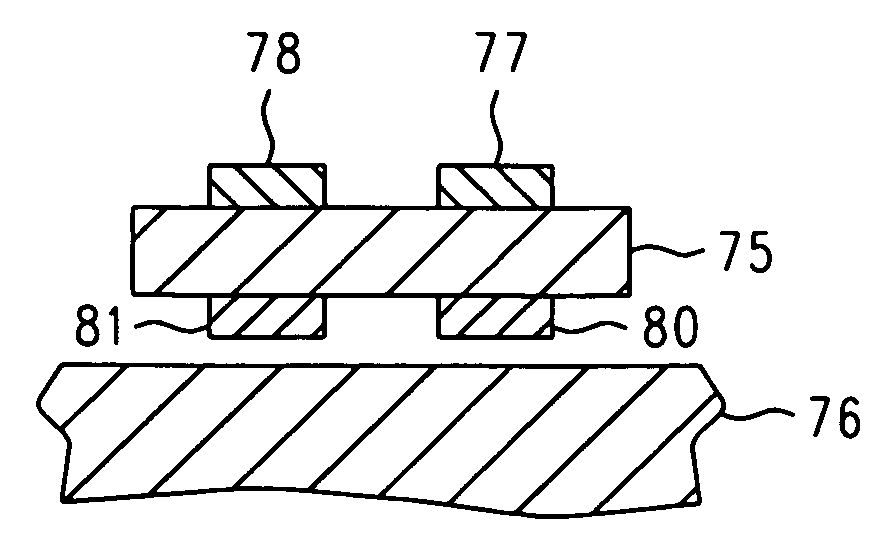
[0047] To assist in the penetration of the arm 2 along the straight path in a direction indicated by arrow 13, the arm 2 may have a rounded nose 4. As an alternative, the rounded nose 4 might shown in this embodiment 1 includes a notch 10 (other alternatives will be presented in due course) whose function would be to increase the ease with which the nose can be compressively warped as it passes between two adjacent solder balls or two adjacent pins, such as 9 and 12.

[0048] To appreciate this notion of compressive warping, note the contacts 7 and 11, respectively formed at the end of the traces 5 and 6. The particular shape of these contacts notwithstanding (these are concave) the maximum distance between the contacts 7 and 11 exceeds the minimum distance between leads 9 and 12. That much is easy to see from the figure. However, it is actually preferred that even when the concavities mate, or almost nearly mate, with the leads 9 and 12, that the contacts 7 and 11 remain in compressio...

embodiment 33

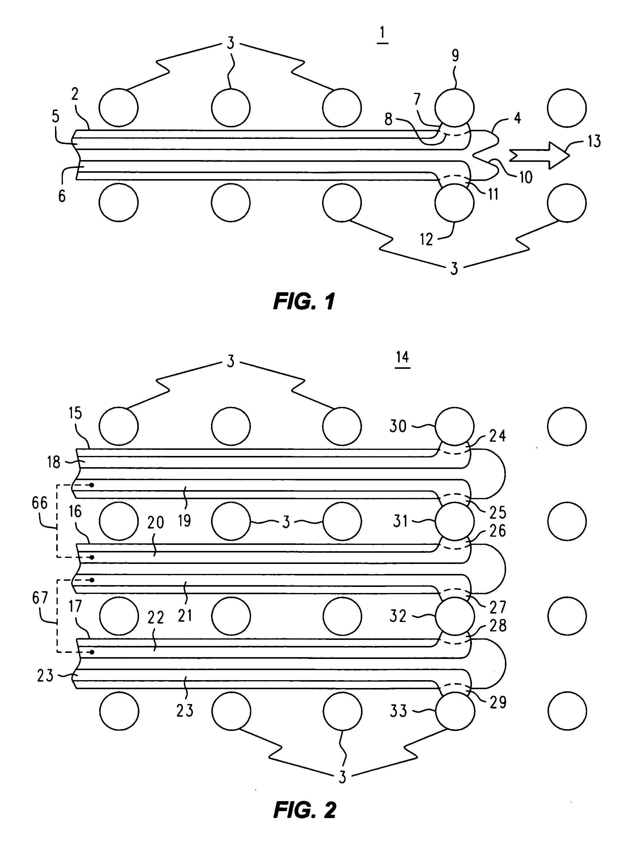
[0056] As it is, the examples of FIGS. 3 and 4 require only four traces on each arm; in the embodiment 33 in FIG. 3 arm 48 has traces 34 and 35 on a ‘top’ side of the arm, which terminate in extended contacts 36 and 37, respectively, while on the ‘bottom’ side of the arm traces 38 and 39 travel to extended contacts 40 and 41, respectively. Contact 44 touches lead 44, contact 37 touches lead 45, both of which are in the same layer of leads. Contacts 40 and 41 touch leads 46 and 47, respectively, both of which are also within a common layer, but which is a different layer than for contacts 36 and 37. Thus the flexible printed circuit substrate for arm 48 need not necessarily in this instance be a multi-layer affair; double sided is sufficient.

[0057] A further difference concerning the embodiment 33 of FIG. 3 is that has an extended nose 49 (which is this instance just so happens to be rounded—it might tapered or pointed as shown in FIG. 4). The nose 49 is extended by the length of reg...

embodiment 85

[0075] We now consider some additional embodiments for an interjacent probe that concern various strategies for touching leads with extended contacts formed upon the arms of an interjacent probe. Refer now to FIG. 7, wherein is shown an embodiment 85, where two arms (there might be only one, or there might be more than two) 86 and 87 each carry a respective single trace (88, 89—temporarily ignore 88a and 89a) that terminates in a corresponding concave contact (90, 91). Contact 90 is to bear against lead 94, while contact 91 is to bear against lead 95. In order to get this to happen through compressive warping, each of arms 86 and 87 includes a respective raised land (92, 93) in the side of the arm opposite the contact (90, 91). These raised lands provide the extra width at the location of the contact to create the compressive warping as land 92 bears against lead 95 and land 93 bears against lead 96.


PUM


Abstract

A probe for an array of interconnecting leads between a PCA and an IC has one or more contacts extending laterally from or plated upon one or more arms formed of a flexible printed circuit, and connected by traces along the arm(s) to a header that itself affords connection to measurement equipment. The flexible printed circuit is thin enough to loosely slide between the top of the PCA or PCB and the bottom of the IC. The arm or arms is / are narrow enough to slide between the adjacent leads forming the array, while the normally flat contacts will successively interfere with, to engage and electrically contact, consecutive layers of leads as the probe is progressively inserted. An arm is not so stiff that it cannot yield by a slight compressive warping as the contacts encounter leads. Indexing may be ‘by feel’ or by visible indicia along a top surface of the probe or by a reticle device that moves over the top of the IC, which then has a pattern of indicia corresponding to lead location. Forming the shape of a Kapton substrate may also include use of a CVL operating in the range of 250 nm to 290 nm for the creation of extended copper contacts by the removal of underlying Kapton. Plating processes may also be used in the fabrication of (non-extended) wrap-around contacts at the edges of the Kapton.

Description

BACKGROUND OF THE INVENTION [0001] VLSI (Very Large Scale Integration) has, on the one hand, produced packaged ICs (Integrated Circuits) containing amounts of circuitry capable of unparalleled functionality. One the other hand, such complex parts typically have a great many signal having corresponding terminals (‘pins’) that require connection to an external environment; often many more than can readily be provided by just pins that could be disposed along the periphery of the part. One of the most common solutions to this problem is to use a BGA (Ball Grid Array) package. [0002] The BGA style of IC packaging utilizes an array (whose outline is typically square, or perhaps rectangular, but any suitable shape is possible) of pads on the underside of the IC part that is to be attached to a PCA (Printed Circuit Assembly). A corresponding (mirror image) array of pads is formed on the PCA at the location that is to receive the IC to be mounted. Some BGAs are solid arrays, with a pad at e...

Claims


Application Information

Patent Timeline
Patent Type & Authority Applications(United States)
IPC IPC(8): G01R31/02
CPCG01R1/04G01R1/073G01R1/067
Inventor HOLCOMBE, BRENT A.LAMERES, BROCK J.JOHNSON, KENNETH W.
Owner AGILENT TECH INC
Why Eureka
Try Eureka