Probe apparatus,wafer inspecting apparatus provided with the probe apparatus and wafer inspecting method

a technology of probe apparatus and probe apparatus, which is applied in the direction of connection contact material, semiconductor/solid-state device testing/measurement, instruments, etc., can solve the problems of inability to stably conduct intended electrical inspection, difficult to surely achieve good electrically connected state, and considerable distance of signal transmission system. , to achieve the effect of high parallelism, good electrically connected sate, and high reliability

Inactive Publication Date: 2007-08-02
ISC CO LTD
View PDF4 Cites 26 Cited by
  • Summary
  • Abstract
  • Description
  • Claims
  • Application Information

AI Technical Summary

Benefits of technology

[0030] According to the probe device of the present invention, upon setting the inspection initial state that the three parties of the circuit board for inspection, the anisotropically conductive connector and the probe card are fixed in a state that the anisotropically conductive connector is pinched by the circuit board for inspection and the circuit board for connection, the undulation of the whole wafer inspection apparatus is adjusted by the parallelism adjusting mechanism to set the inspection initial state in a state that the three parties of the circuit board for inspection, the probe card and the wafer that is an object of inspection have an extremely high parallelism, so that displacement of the circuit board for inspection or the circuit board for connection in a direction that a clearance between the circuit board for inspection and the circuit board for connection becomes great is prohibited by the location-varying mechanism, and the respective contacts in the contact member and the respective electrodes to be inspected formed on the wafer are electrically connected while retaining the high parallelism to the wafer over the whole probe device. As a result, a necessary electrically connected state can be stably attained under a small load.
[0031] When the contact member in the probe card is constructed by that equipped with the anisotropically conductive sheet, in which a plurality of conductive parts for connection each extending in the thickness-wise direction thereof are mutually insulated by an insulating part, irregularities-absorbing property by the anisotropically conductive connector is basically obtained, and moreover the irregularities-absorbing property of the anisotropically conductive sheet itself in the contact member is achieved by being pressurized while retaining the high parallelism to the wafer over the whole probe device in a state that the irregularities-absorbing property is kept as much as possible, so that a good electrically connected state can be stably attained with higher certainty under a small load.
[0032] According to the wafer inspection apparatus of the present invention, since it is equipped with the probe device described-above, a good electrically connected sate can be stably attained between respective electrodes to be inspected formed on the wafer and respective contacts of the contact member under a small load. Accordingly, the intended electrical inspection can be surely conducted with high reliability.
[0033] According to the wafer inspection method of the present invention, since respective electrodes to be inspected formed on the wafer and respective contacts of the contact member are electrically connected in a state that the undulation of the whole wafer inspection apparatus is corrected by the parallelism adjusting mechanism, the intended electrical inspection can be surely conducted with high reliability.

Problems solved by technology

However, such a wafer inspection apparatus as shown in FIG. 17 involves such problems as described below.
Accordingly, the wafer inspection apparatus involves a problem that the mere movement of the wafer tray 96 upward to pressurize the wafer W makes it difficult to surely attain a good electrically connected state between the respective contacts in the contact member 95 and the electrodes to be inspected in the wafer W because, for example, the contact member 95 becomes a state coming into contact with the wafer W at only one side due to the undulation of the whole wafer inspection apparatus, and after all, intended electrical inspection cannot be stably conducted.
Since the connecting pins 86 in the wafer inspection apparatus of the above-described construction require to have a considerably long length, a distance of a signal transmission system becomes considerably long, so that a problem arises that the apparatus is difficult to be adapted to electrical inspection as to high functional integrated circuits to which high-speed processing is required.

Method used


Image

  • Probe apparatus,wafer inspecting apparatus provided with the probe apparatus and wafer inspecting method
  • Probe apparatus,wafer inspecting apparatus provided with the probe apparatus and wafer inspecting method
  • Probe apparatus,wafer inspecting apparatus provided with the probe apparatus and wafer inspecting method

Examples


example 1

(1) Production of Wafer for Evaluation:

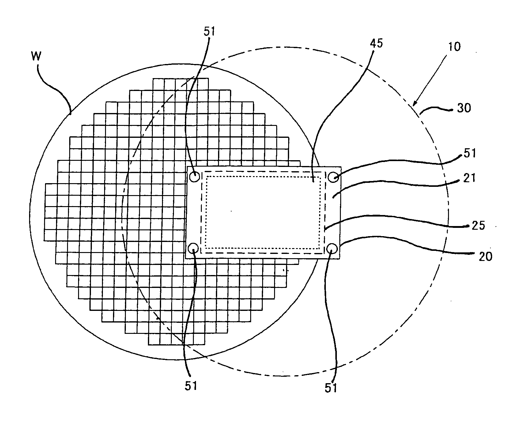
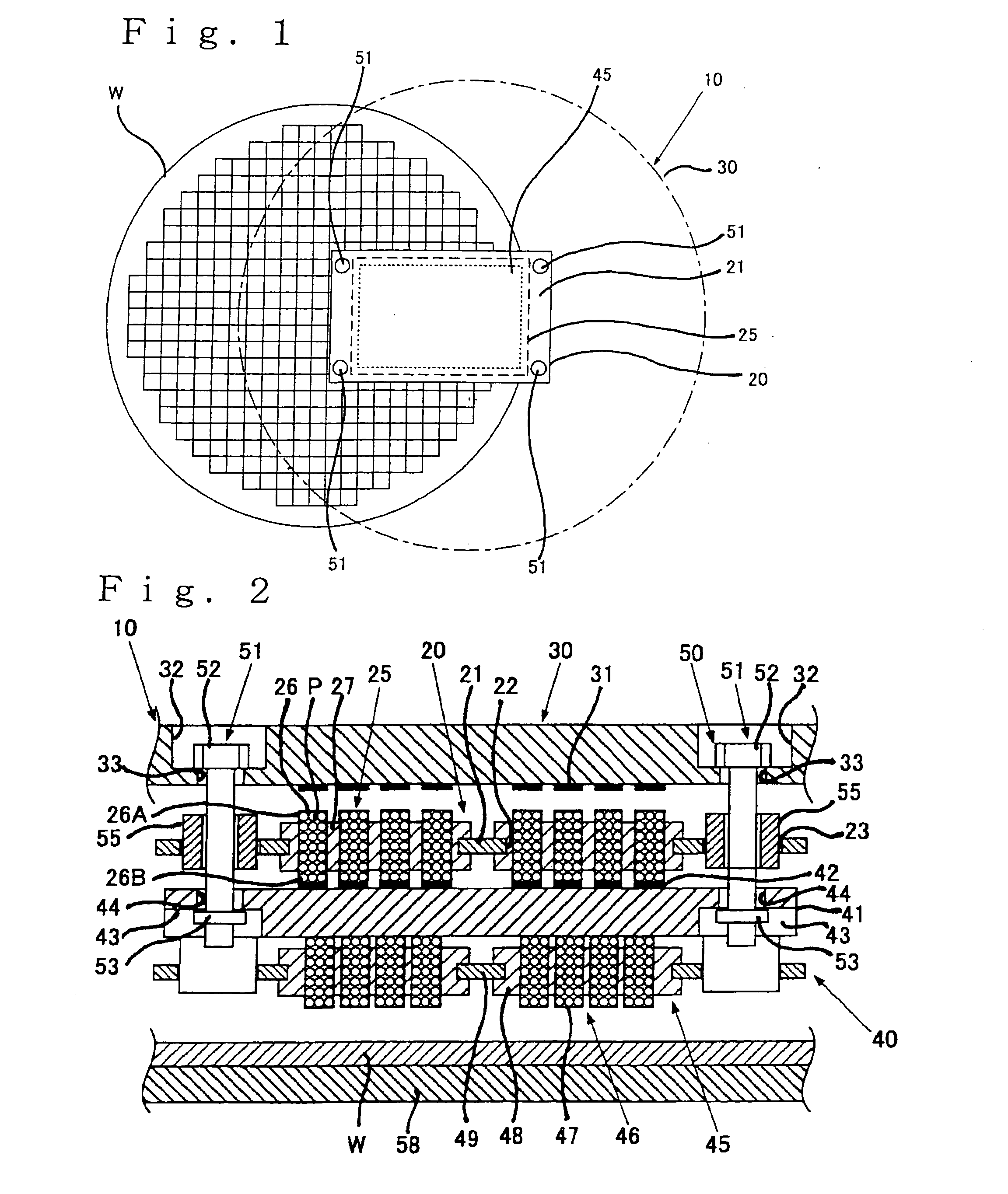
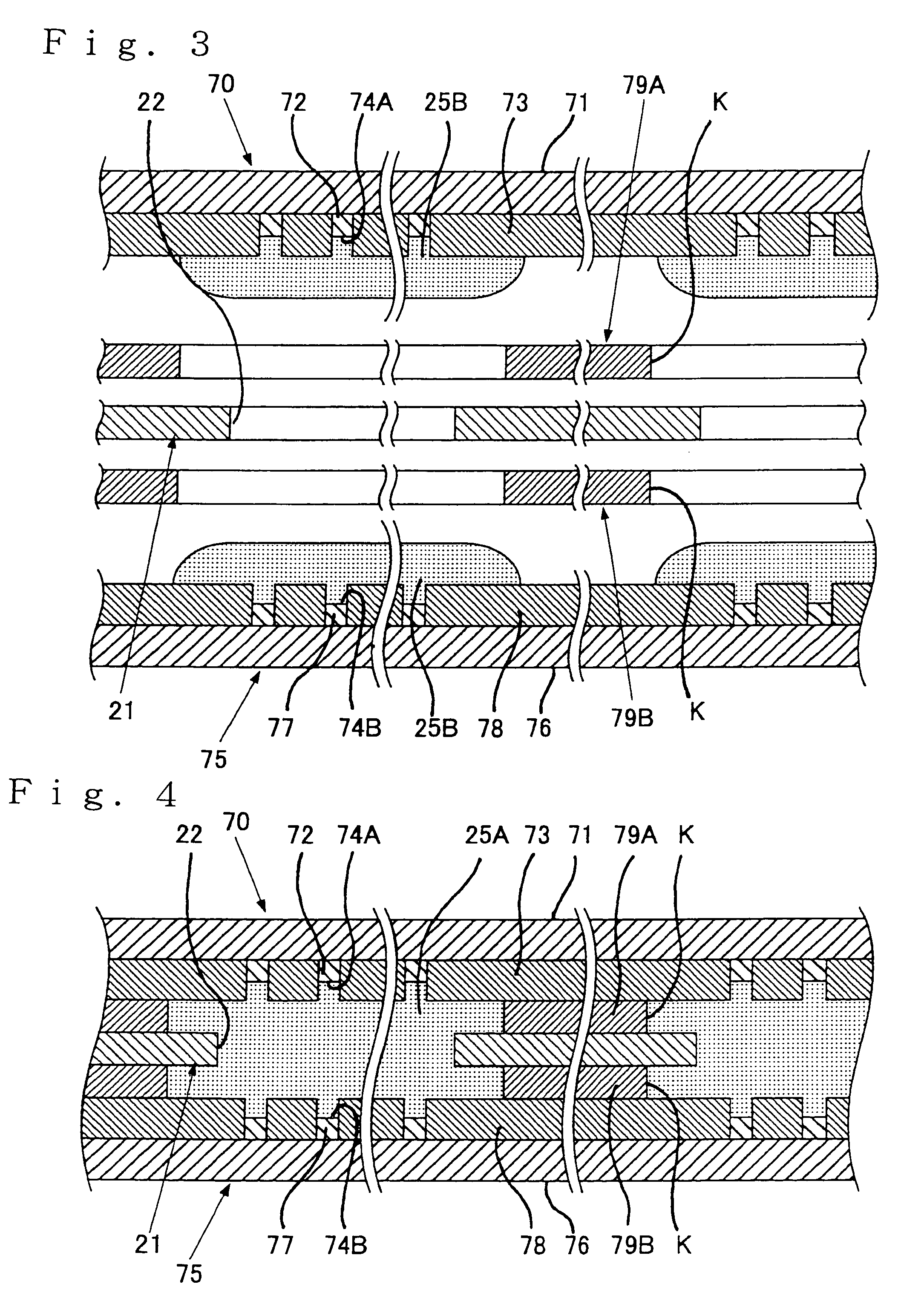
[0251] On a wafer made of silicon (coefficient of linear thermal expansion: 3.3×10⁻⁶ / K) and having a diameter of 8 inches, sixty-four (64) rectangular integrated circuits in total, which each had dimensions of 11,000 μm in a lateral direction and 6,000 μm in a vertical direction, were formed so as to arrange eight (8) by eight (8) integrated circuits in vertical and lateral directions. Each of the integrated circuits formed on the wafer has a region of electrodes to be inspected at its center. In this region of the electrodes to be inspected, sixty (60) electrodes to be inspected each composed of copper and plated with gold on the surfaces thereof are arranged at a pitch of 120 μm in a line in the lateral direction. Every two electrodes among the sixty (60) electrodes to be inspected are electrically connected to each other. Each of the electrodes to be inspected has dimensions of 80 μm in a lateral direction and 170 μm in a vertical directio...

example 2

[0290] A probe device having the same construction as that produced in Example 1 except that spacers of the construction shown below were used as the spacers for regulating a deformation quantity in Example 1, and such spacers were arranged on both surfaces of the frame plate in the anisotropically conductive connector for adjusting undulation was produced (cf. FIG. 5).

[Construction of Spacer]

[0291] The spacers are constructed by a rectangular frame-like plate part having opening in regions corresponding to regions, in which the elastic anisotropically conductive films in the anisotropically conductive connector for adjusting undulation have been formed, and a plurality of finely projected portions composed of an elastic substance and formed on both surfaces of this plate part.

[0292] The plate part is composed of stainless steel and having a thickness of 50 μm. The finely projected portions are composed of silicone rubber and in a columnar form that the diameter is 50 μm, and the...


PUM


Abstract

A probe device including a circuit board for inspection having a great number of inspection electrodes, a probe card having a circuit board for connection having a great number of terminal electrodes and a contact member, an anisotropically conductive connector arranged between the circuit board for inspection and the circuit board for connection and electrically connecting the respective inspection electrodes to the respective terminal electrodes, and a parallelism adjusting mechanism for adjusting a parallelism of the circuit board for inspection and the circuit board for connection to the wafer. The parallelism adjusting mechanism includes a location-varying mechanism, which relatively displaces the circuit board for inspection or the circuit board for connection in the thickness-wise direction of the anisotropically conductive connector. A wafer inspection apparatus can include the probe device.

Description

TECHNICAL FIELD [0001] The present invention relates to a wafer inspection apparatus and a wafer inspection method carried out in this wafer inspection apparatus, and a probe device suitable for use in this wafer inspection apparatus, and particularly to a wafer inspection apparatus and a wafer inspection method for collectively conducting a probe test as to a part or all of a great number of integrated circuits formed on a wafer, or a wafer inspection apparatus and a wafer inspection method for collectively conducting a burn-in test as to a part or all of a great number of integrated circuits formed on a wafer, and a probe device suitable for use in these wafer inspection apparatus. BACKGROUND ART [0002] In the production process of semiconductor integrated circuit devices, after a great number of integrated circuits are formed on a wafer, a probe test is generally conducted as to each of these integrated circuits. This wafer is then cut, thereby forming semiconductor chips. Such s...

Claims


Application Information

Patent Timeline
Patent Type & Authority Applications(United States)
IPC IPC(8): H01R4/58G01R1/06G01R1/073G01R31/28H01L21/66
CPCG01R1/07314G01R1/07378G01R1/07371G01R1/07364H01L22/00
Inventor IGARASHI, HISAOSATO, KATSUMIINOUE, KAZUO
Owner ISC CO LTD
Why Eureka
Try Eureka